
Prober Shuttle PS4 @ Phenom XL
Four-probe in-situ electrical nanoprobing inside the Phenom XL desktop SEM, built on the ultra-flat MM4 manipulator platform.
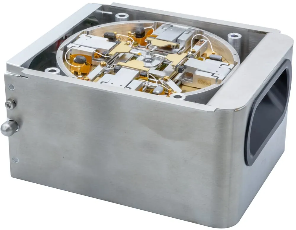
Four probes, one feedthrough#
The Prober Shuttle PS4 @ Phenom XL puts high-precision in-situ electrical nanoprobing inside a desktop SEM. It is built on the MM4 — an ultra-flat three-axis micromanipulator that resolves motion below 0.05 nm with drift held to 1 nm/min — and ships configured with two or four MM4s, optionally paired with an ultra-flat two- or three-axis substage.
Why four without a substage#
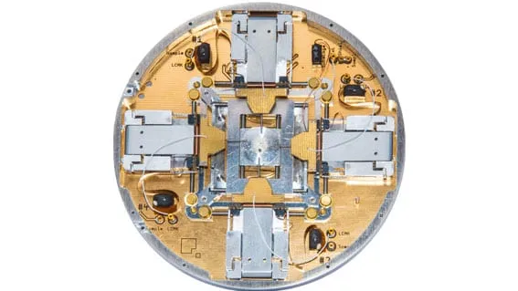
The Phenom XL’s vacuum feedthrough carries a finite number of contacts, which caps the shuttle at four micromanipulators; adding the substage drops that to three. For most nanoprobing work, a four-probe setup without the substage is the practical choice — and the one shown assembled above, with all four probe leads converging on the shuttle’s central gold contact disc.
Built for low-current work#
Each probe reaches down to 25 fA at 1 Hz, with insulation leakage below 50 fA/V and signal-conductor resistance under 5 Ω — enough headroom to run the Advanced Probing Tools suite, including the Live Contact Tester and Electron Beam Induced Current (EBIC) imaging.
Gallery
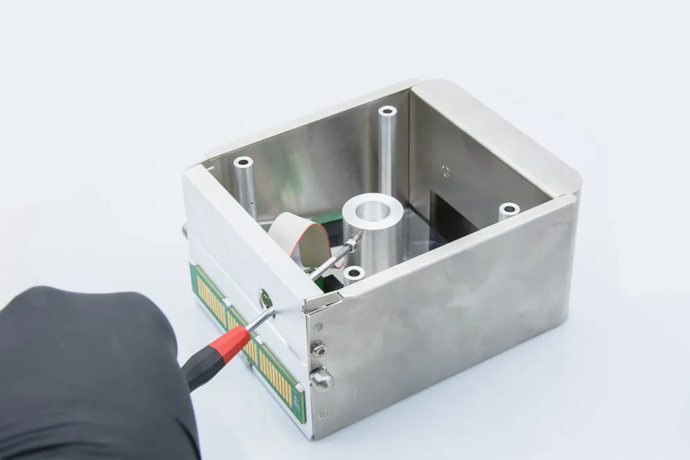
The shuttle body before the rotary sample carrier is seated. 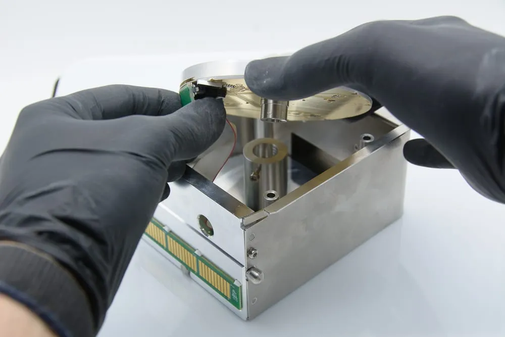
Seating the gold flex-circuit carrier that routes signal to each probe. 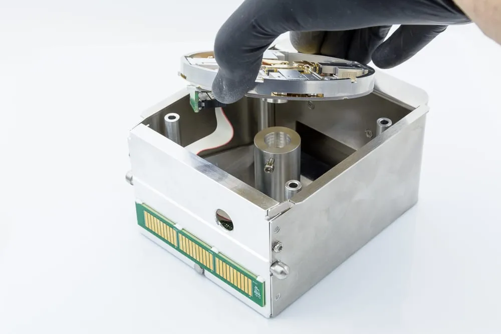
Four MM4 probe leads converging on the central gold contact disc. 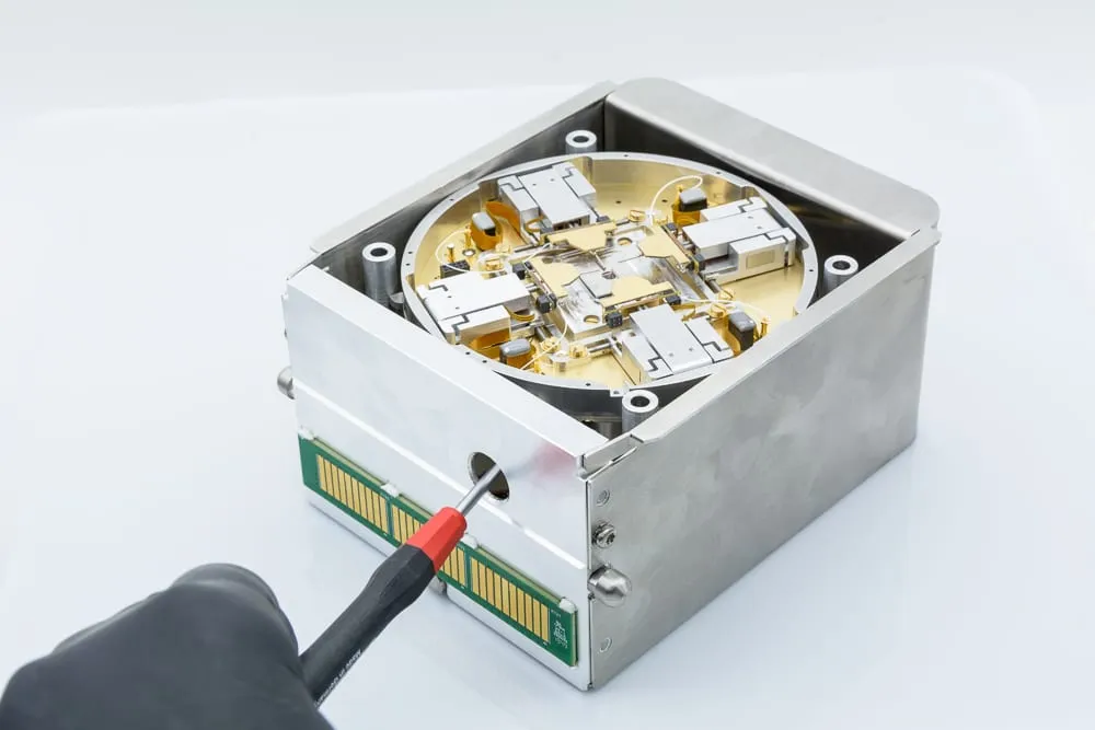
Closed and ready for load-lock transfer into the Phenom XL chamber.
Technical data
Overview
- Total height
- 10 mm
- Total width
- 100 mm
- Maximum sample area
- 20 mm × 20 mm
- Maximum sample height
- 10 mm (depending on sample area and load-lock dimensions)
- Weight
- 100 g + SEM/FIB dovetail
Micromanipulators
- Operating range A
- 9 mm
- Operating range B
- 90°
- Operating range C
- 5 mm
- Resolution A
- < 0.05 nm
- Resolution B
- < 0.5 nm
- Resolution C
- < 0.05 nm
- Drift
- 1 nm/min
Low-capacitance, low-current measurements
- Noise
- 25 fA @ 1 Hz
- Insulation leakage current
- < 50 fA/V
- Signal conductor resistance
- < 5 Ω
- Maximum voltage
- 100 V
- Maximum current
- 100 mA
Advantages
Clean, non-magnetic build
- Non-magnetic design
- Ready for 5 nm and beyond
- Clean cable management from flange to rack
Advanced probing ready
- Low-current, low-capacitance measurement capability
- Fully compatible with the Advanced Probing Tools hardware and software suite
- Includes the Live Contact Tester and Electron Beam Induced Current (EBIC) imaging modules
Related products & accessories
Talk to an application engineer
Tell us your sample and your microscope — we’ll walk you through the workflow and route you to the right regional team.