
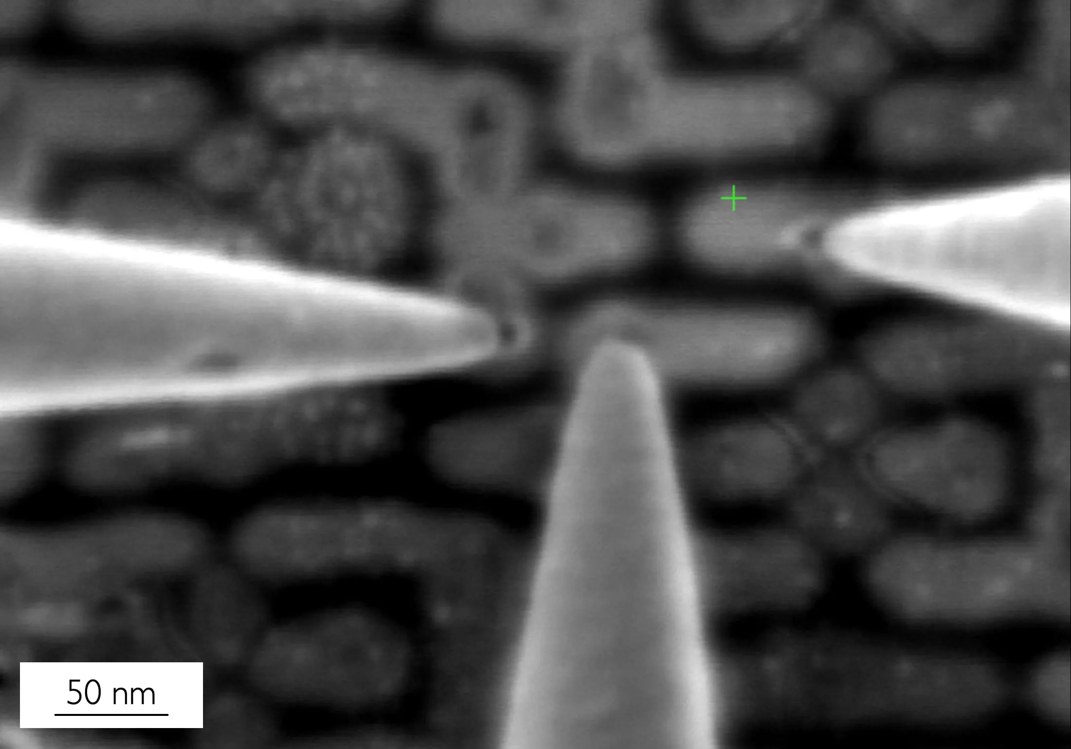
Nanoprobing
Land ultra-fine needles on individual transistors to measure their electrical behaviour at the most advanced nodes.
Measuring the I–V curve of a single transistor is routine, until the transistor shrinks to a few tens of nanometres. Then it becomes one of the hardest measurements in the failure-analysis lab, demanding probes with sub-nanometre positioning and the mechanical stability to hold contact for the measurement.
Kleindiek nanoprobing lands ultra-fine needles on individual device terminals inside your SEM or FIB/SEM, with the throughput a busy FA lab needs. The articles here go deeper: the introduction explains the measurement and the hardware, the current-imaging techniques show how to locate a defect before probing it, and the video series shows systems at work.
Datasheets & application notes
Articles & videos
Short, focused reads and in-microscope footage — start with the introduction or jump to a technique.
Technical deep-dives
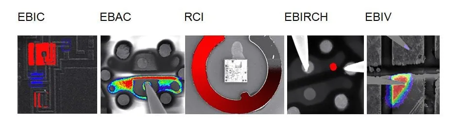
Current imaging for failure analysis
Electron-beam current-imaging techniques that localize faults before you probe.
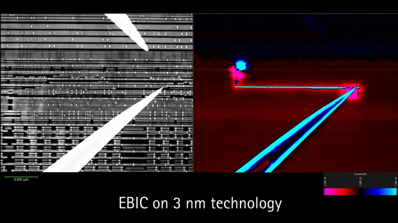
EBIC — Electron-Beam-Induced Current
Mapping where a device collects beam-generated carriers, to image p–n junctions, depletion regions and recombination sites.
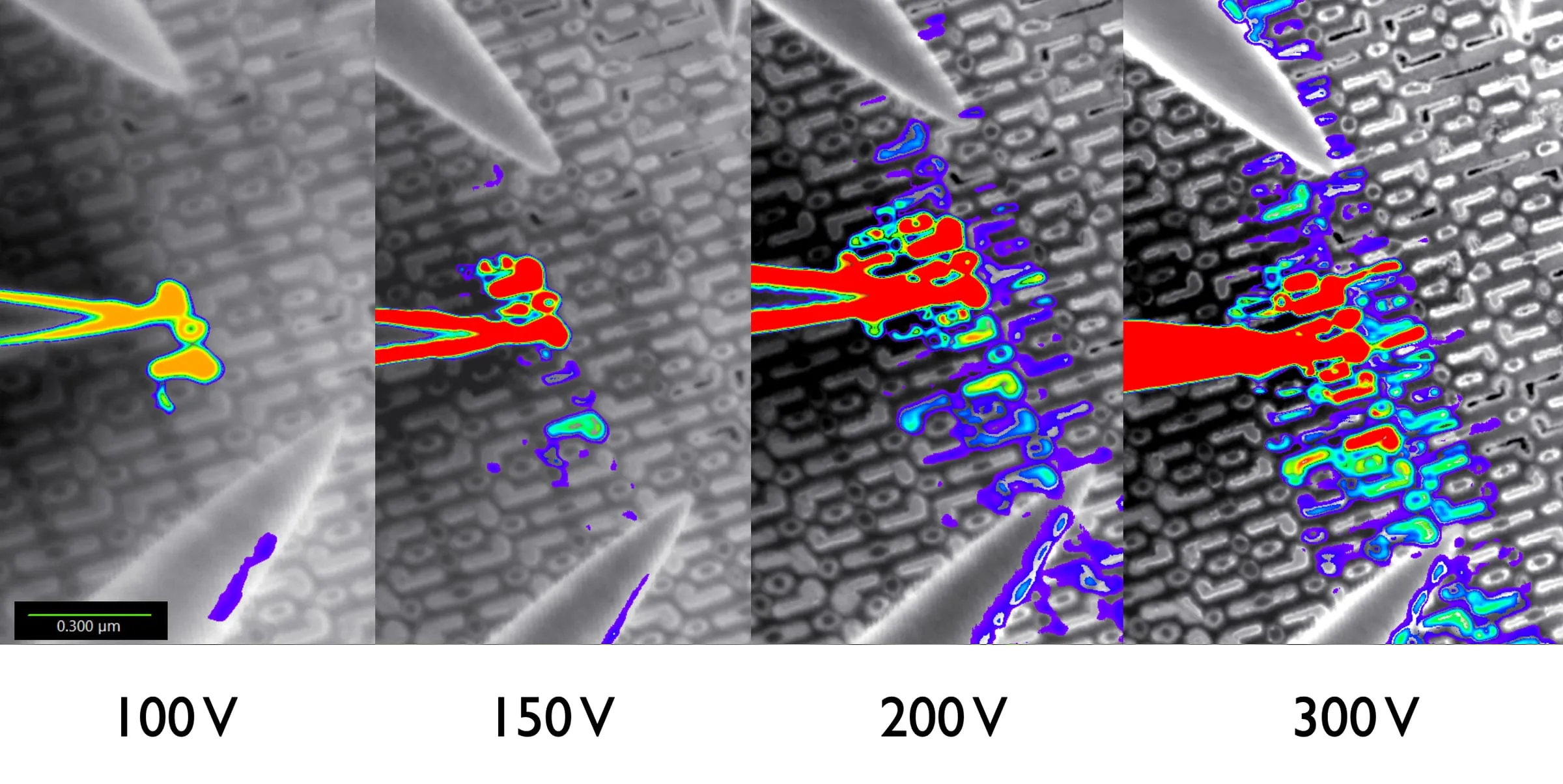
EBAC — Electron-Beam Absorbed Current
Tracing conductive paths and finding opens in interconnects, with no bias applied to the device.
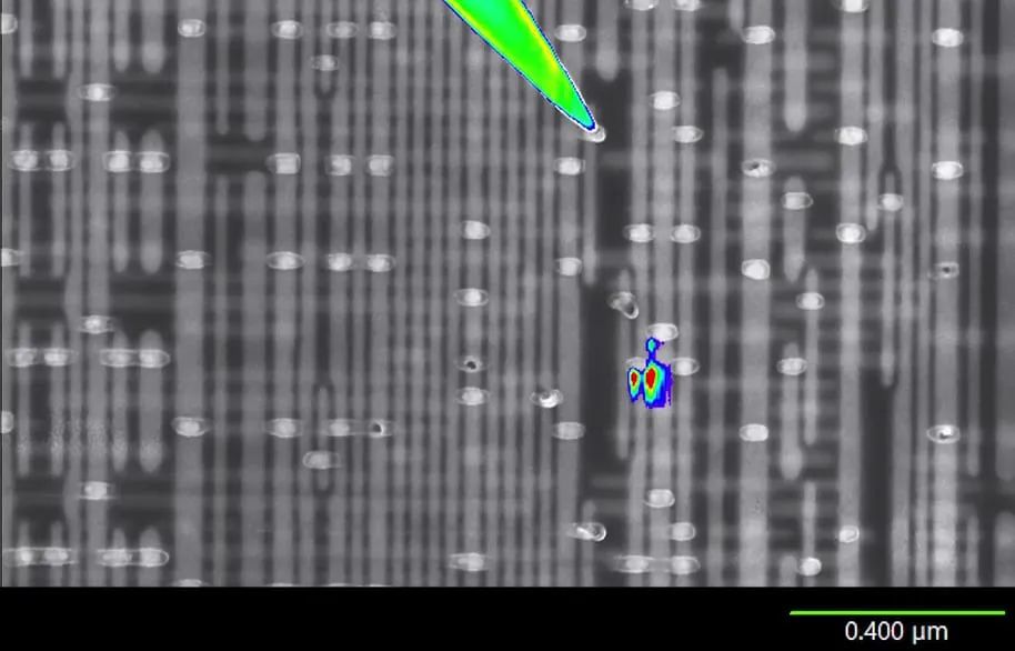
RCI — Resistive Contrast Imaging
Two-contact current-division imaging that reveals the resistance distribution along a net.
EBIRCH — Electron-Beam-Induced Resistance Change
Biased, AC current imaging that lights up resistive and leaky defects as bright spots.
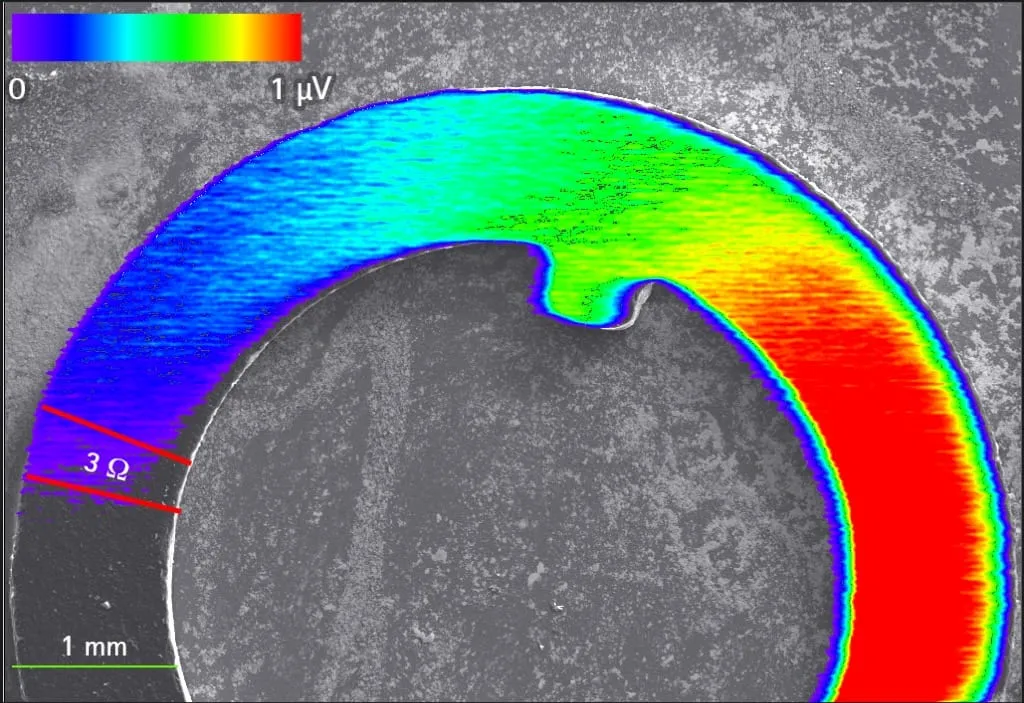
EBIV — Electron-Beam-Induced Voltage
Reading the beam-induced voltage to reach high-impedance and floating nodes that current maps miss.
Products used
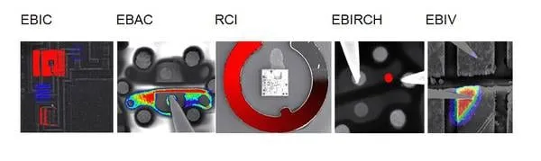
EBIC Amplifier
A low-noise current amplifier that turns the electron beam into a defect-mapping tool — EBIC, EBAC, RCI, EBIRCH and EBIV from a single unit.
View product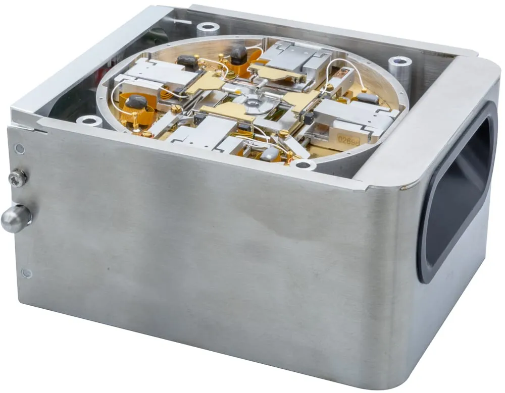
Prober Shuttle PS4 @ Phenom XL
Four-probe in-situ electrical nanoprobing inside the Phenom XL desktop SEM, built on the ultra-flat MM4 manipulator platform.
View product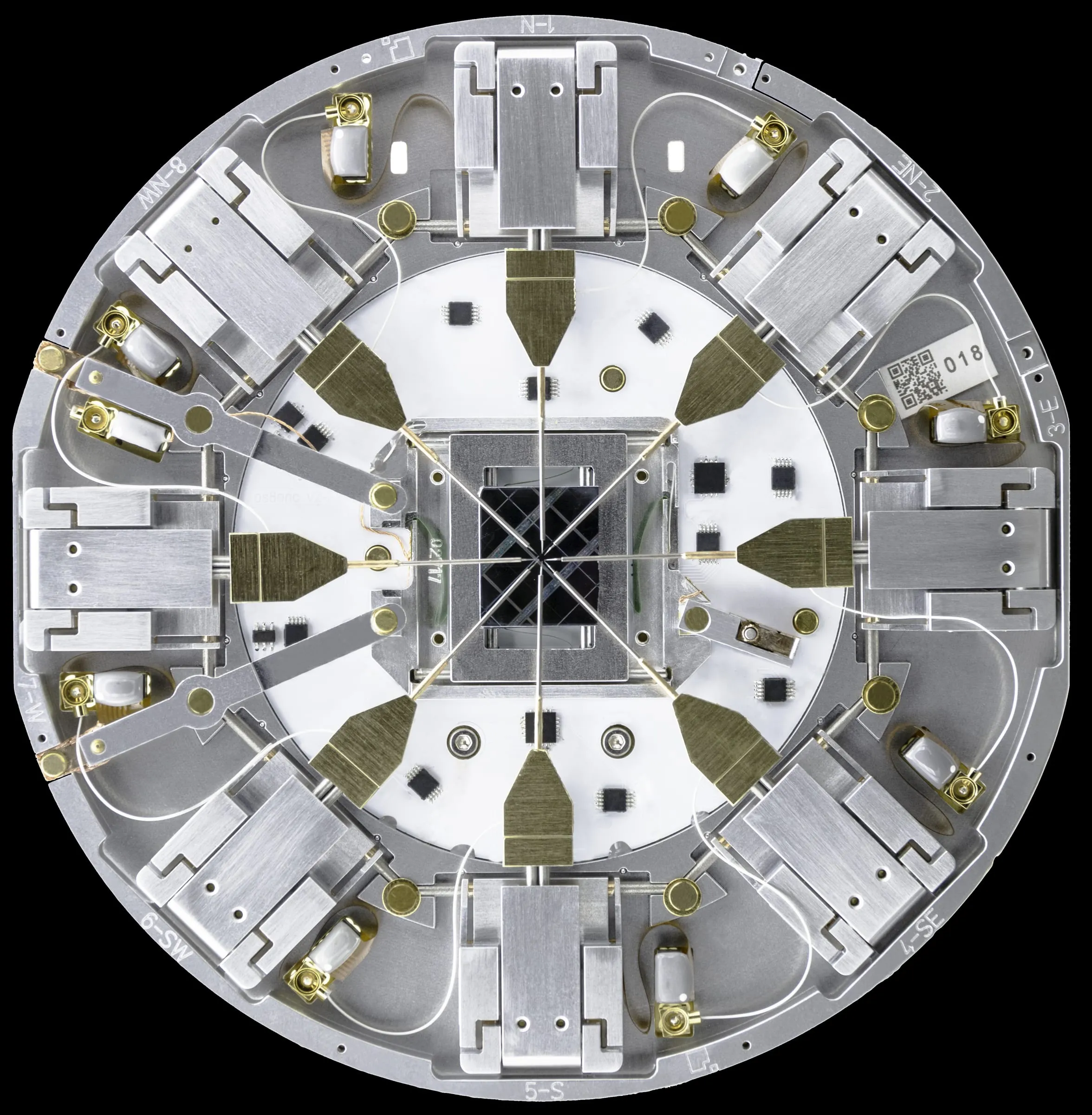
Prober Shuttle PS8e
A compact, fully integrated nanoprobing system — now encoded for automatic probe pre-alignment. Optimized for the 3 nm node and beyond.
View product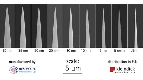
Mesoscope Probe Tips
High-end tungsten probe tips with radii from 250 nm down to 5 nm — ready to probe straight from the pack.
View product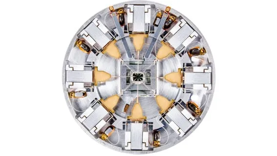
Prober Shuttle PS8
High-precision in-situ electrical nanoprobing with up to eight ultra-flat MM4 manipulators — for advanced-node failure analysis.
View product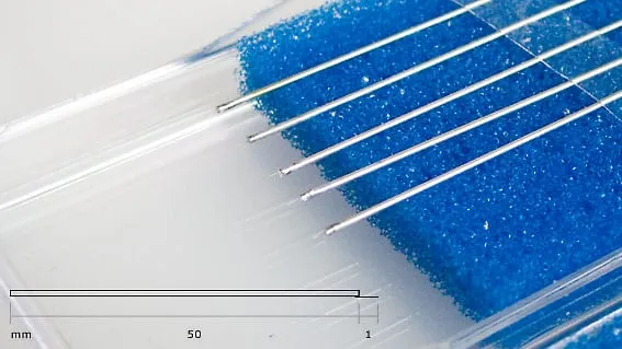
PicoProbe Tips
Tungsten probe tips for everyday probing — most commonly 100 nm radius, packaged under protective atmosphere.
View product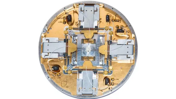
Prober Shuttle PS4
A compact two- or four-probe nanoprobing system for in-situ electrical characterization at advanced nodes.
View product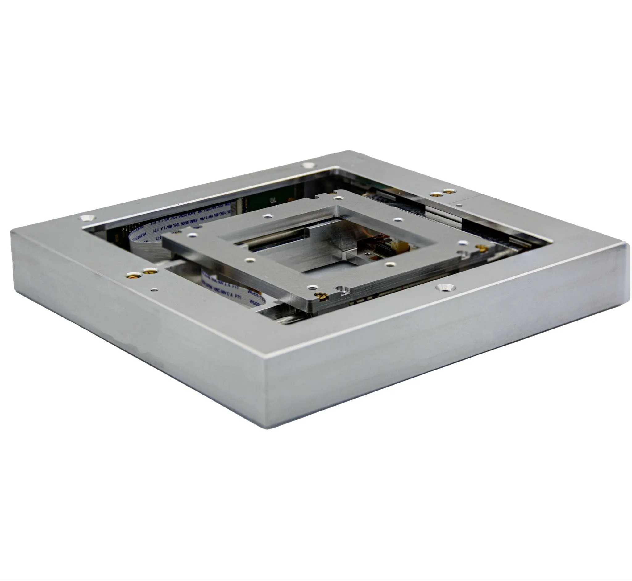
LT14030
A 30 mm-travel encoded linear table with dual-encoder yaw compensation — an economical alternative to laser-interferometer stages.
View product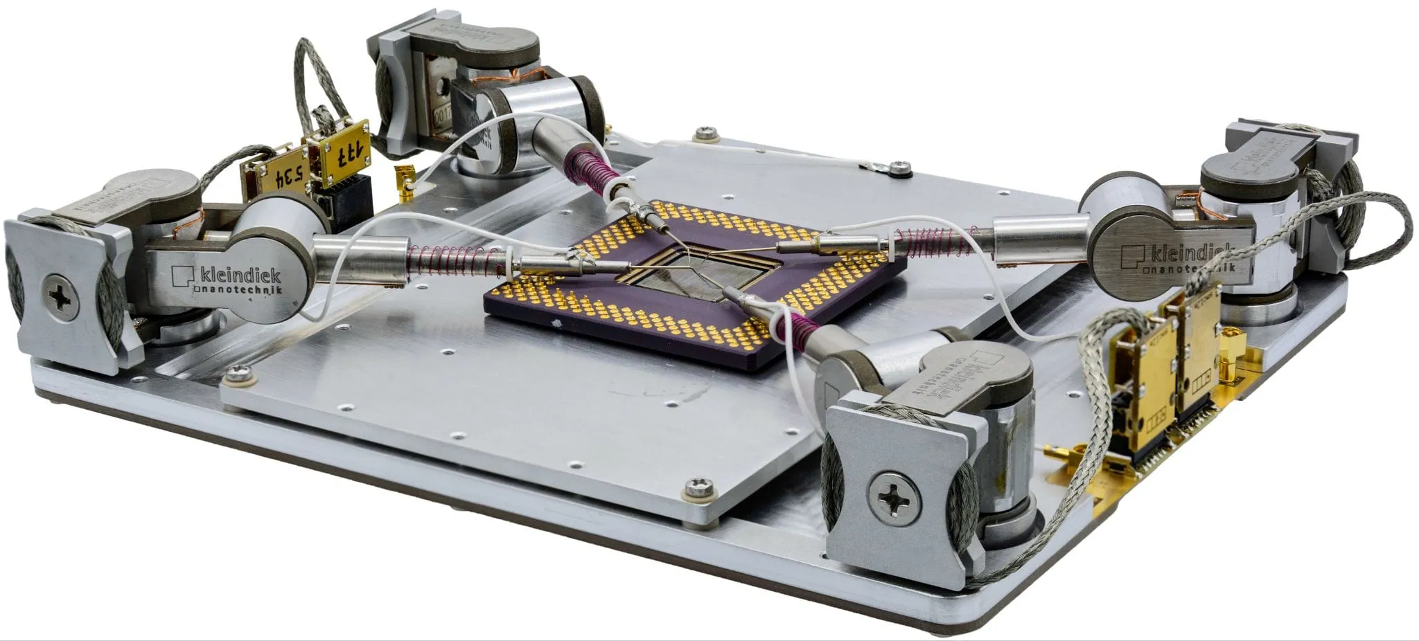
NW4
A load-lock platform hosting up to four MM3A-EM manipulators — nanoprobing and failure analysis on large substrates up to 120 × 120 mm.
View product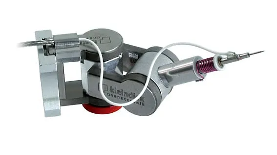
Probe-Tip Holder LCMK
A low-noise, low-resistance probe-tip holder that turns a Kleindiek manipulator into a precision nanoprober — resolving currents down to 3 fA.
View product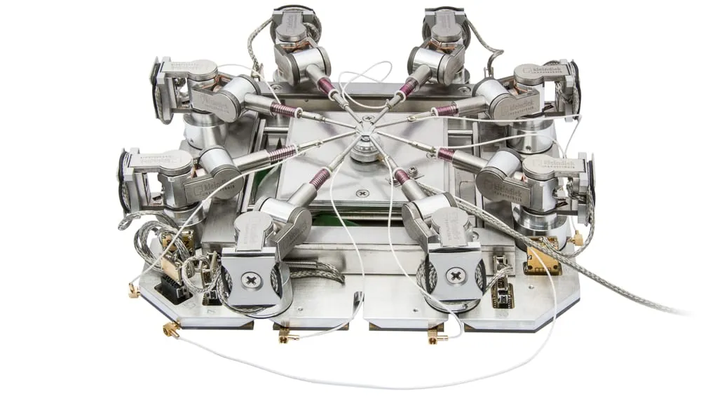
ProbeWorkstation+
Up to eight manipulators, a roof-mounted prober and a 30 mm substage — a complete in-SEM probe station, installed or removed in 60 seconds.
View product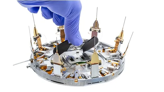
Heating & Cooling Stage for PS8
A heated/cooled stub for the Prober Shuttle PS8 — regulate sample temperature from −20 °C to +150 °C during probing, water-cooling-free.
View product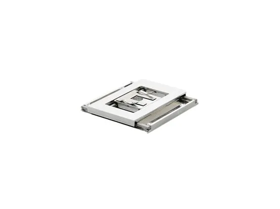
SFLT3310
An ultra-low-profile 3.8 mm-tall piezo linear table — smooth XY motion in the tightest spaces, ideal paired with the Prober Shuttle.
View productRelated publications
Magnetic energies of single submicron permalloy rectangles determined via magnetotransport
DOI 10.1103/PhysRevB.80.134415Exploring the conduction in atomic-sized metallic constrictions created by controlled ion etching
DOI 10.1088/0957-4484/19/41/415302Accurate electrical testing of individual gold nanowires by in situ scanning electron microscope nanomanipulators
DOI 10.1063/1.3005423Integrated setup for the fabrication and measurement of magnetoresistive nanoconstrictions in ultrahigh vacuum
DOI 10.1063/1.29816933D failure analysis in depth profiles of sequentially made FIB cuts
DOI 10.1016/j.microrel.2007.07.032Establishing Ohmic contacts for in situ current–voltage characteristic measurements on a carbon nanotube inside the scanning electron microscope
DOI 10.1088/0957-4484/17/4/041Development and performance of the nanoworkbench: A four tip STM for conductivity measurements down to submicrometer scales
DOI 10.1063/1.1878213Performing probe experiments in the SEM
DOI 10.1016/j.micron.2003.12.005Talk to an application engineer
Tell us your sample and your microscope — we’ll walk you through the workflow and route you to the right regional team.