Why it’s hard#
At the leading edge a transistor is only a few tens of nanometres across. To measure one you have to place several probes, each finer than the features themselves, and hold them steady while you sweep voltages. Any drift or backlash and the contact is lost. Beam-sensitive devices add another constraint: you often have to work at very low acceleration voltage, where seeing and landing probes is hardest.
How nanoprobing works#
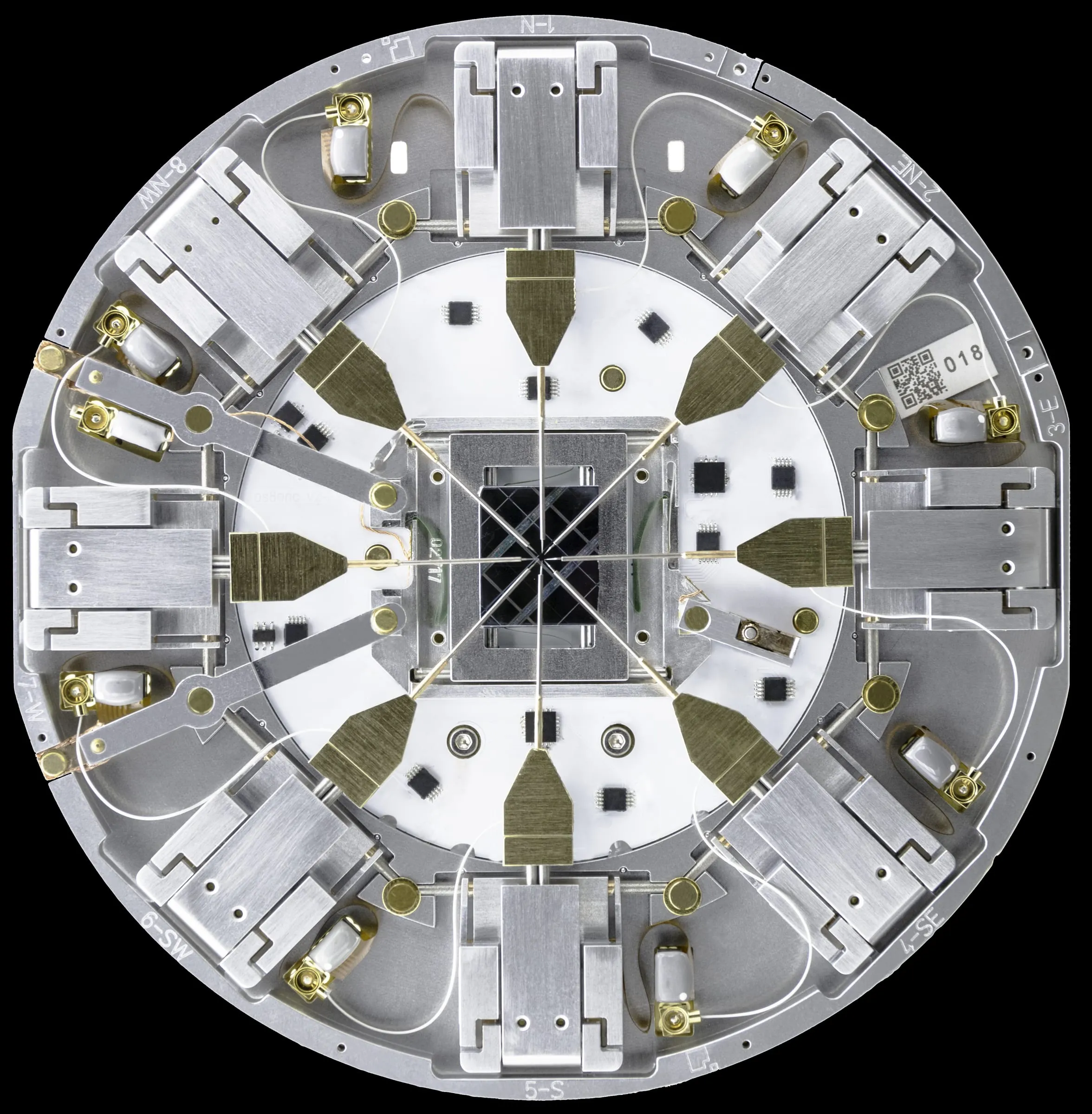
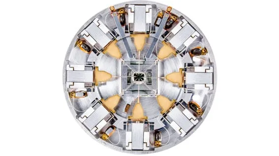
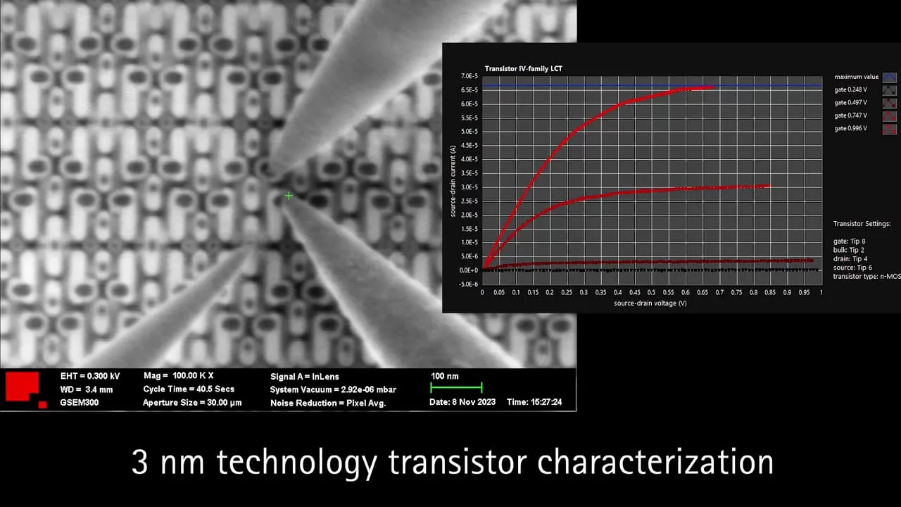
A Prober Shuttle carries several ultra-flat manipulators on a single stage that drops onto your microscope’s sample stage. Each manipulator lands a sub-nanometre-precise needle on a device terminal; low-current, low-capacitance signal paths then capture the tiny currents of advanced-node devices, so you can record full I–V families in situ.
Beyond DC probing#
The same platform supports current-imaging techniques (EBIC, EBAC, EBIRCH) to map electrical activity and localize faults before you probe. On beam-sensitive nodes, encoded systems such as the PS8e pre-align the probes automatically at low kV.
From here, read how current imaging works, or watch the systems at work in the video series.