Where the built-in field separates the carriers#
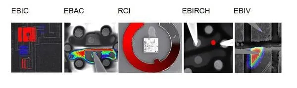
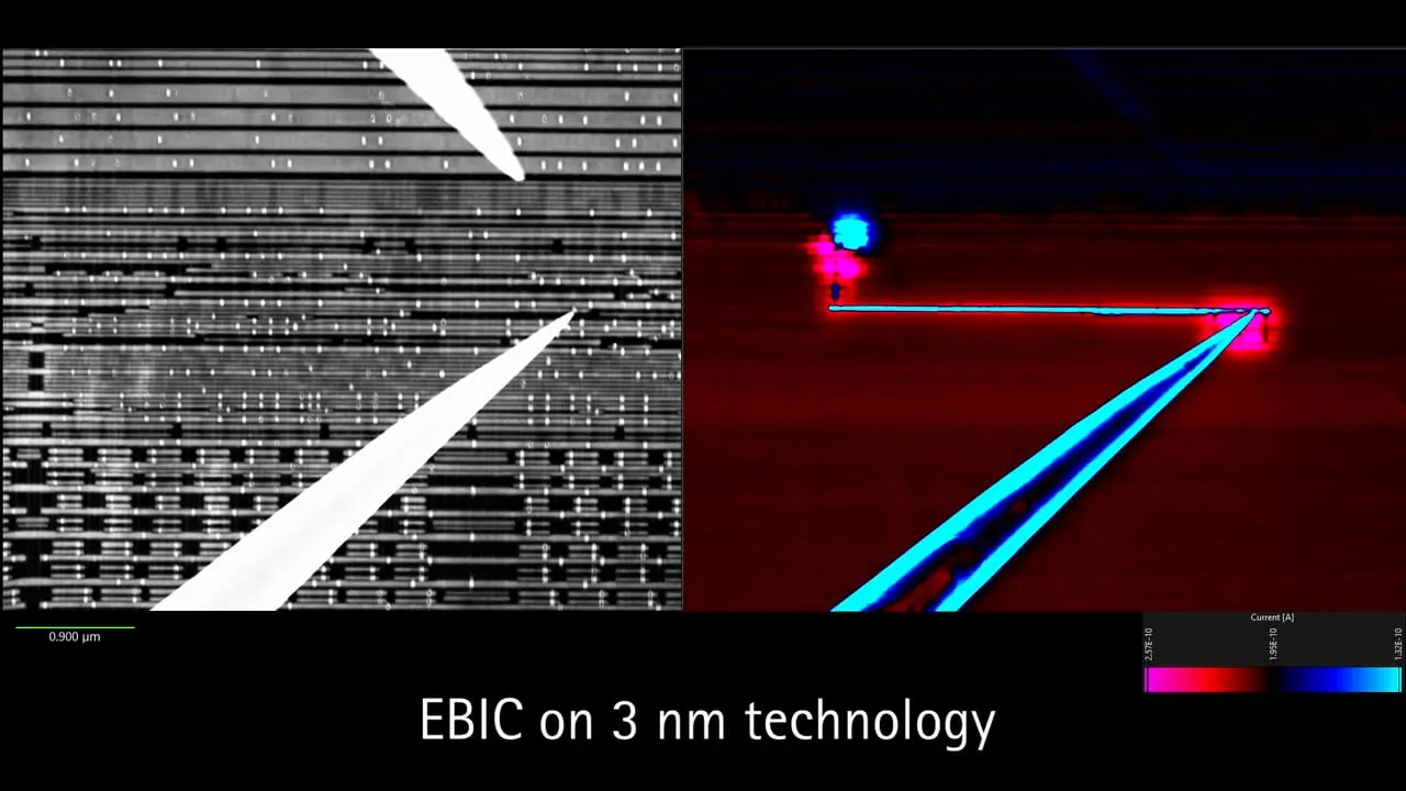
In EBIC, the focused electron beam generates electron–hole pairs in the semiconductor. Wherever a built-in electric field exists, such as a p–n junction, a Schottky contact or a depletion region, those carriers are separated and swept out as a current. Reading that current while the beam scans builds a map in which active junctions and charge-collecting regions stand out brightly, while recombination-active defects such as dislocations show up as dark contrast.
Passivation stays on, depth is yours to choose#
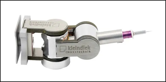
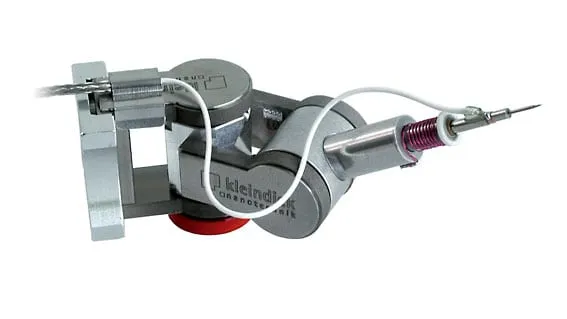
Probes carried by the manipulators contact the device, the collected current goes to the EBIC amplifier, and its output drives the microscope’s video input, producing a greyscale current map registered to the secondary-electron image. The passivation layer can stay in place, and tuning the beam’s accelerating voltage changes the penetration depth, so junctions can be examined at chosen depths below the surface.
From junction depth to solar-cell quality#
Locating and characterizing p–n junctions, checking junction depth and uniformity, finding recombination-active defects, and judging the material quality of solar cells and power devices, all without removing passivation or damaging the device.