
MM3A-EM
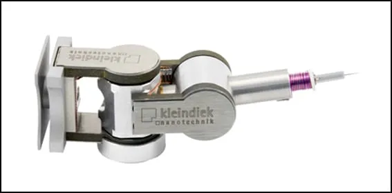
The industry-standard spherical micromanipulator — the platform every Kleindiek plug-in tool attaches to, with 3000+ units in the field.
Two decades, one industry standard#
Refined for electron microscopy over more than twenty years, the MM3A-EM is the OEM and retrofit standard across SEM, FIB and combined instruments — with well over 3000 units in the field. Each unit passes a one-year endurance test before it ships, and in production use drift stays below 1 nm/min, so a probe placed at the start of a long acquisition is still where you left it at the end.
Give your microscope a hand: use the MM3A-EM to add new capabilities and functionality to your instrument.
No blind axis, no stage swap#
The spherical Nanomotor® mechanism folds coarse positioning and sub-nanometre fine motion into a single drive — 0.5 nm on axis A, 0.2 nm on B, 0.05 nm on C — with no backlash and no “blind axis” the way cartesian stages have. That geometry delivers 100 cm³ of working volume from a body that mounts on one M4 tapped hole, and its compact construction keeps resonance frequencies high, so the tip stays put under the beam.
A hub for the whole toolkit#
Swap probe tips by hand between samples, then attach any of seven Kleindiek plug-in tools — microgripper, rotational wrist, force-measurement system and more. Ready-made interfacing covers Zeiss, FEI, Hitachi and Jeol instruments, door to load-lock mounts. At the National University of Singapore, two MM3A-EMs isolated a single carbon nanotube from a bundle and bent it through several micronewtons of force without breaking it.
Gallery
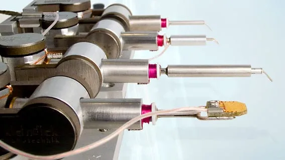
Different tip options mounted side by side, from a fine tungsten point to a sample-holding tip. 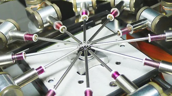
Multiple manipulators run around one sample without fouling each other. 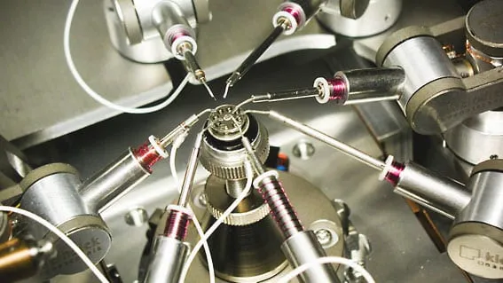
Probe tips closing in on a sample stub from several angles at once. 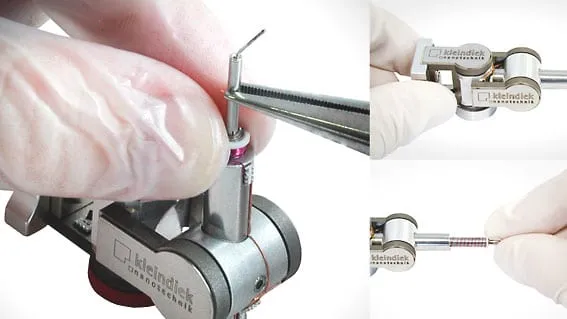
Tip exchange by hand — no tools, no venting the chamber.
Technical data
Motion
- Range — A & B
- 240°
- Range — C
- 12 mm
- Speed — A & B
- up to 10 mm/s
- Speed — C
- up to 2 mm/s
- Holding torque
- 3 – 4 Nmm
- Holding force
- 1 N
- Lift — B
- 5 g
Resolution
- Axis A
- 0.5 nm (7 nrad)
- Axis B
- 0.2 nm (7 nrad)
- Axis C
- 0.05 nm
Dimensions
- Length
- 62.1 mm
- Width
- 20.4 mm
- Height
- 25.4 mm
- Weight
- 45 g
- Mounting
- M4 tapped hole
- Material
- Stainless steel, aluminium
Electrical & environment
- Probing current
- 10 nA – 100 mA
- Max. probing voltage
- 100 V
- Signal resistance
- 7.0 Ω
- Temperature — standard
- 273 K – 353 K
- Temperature — UHV version
- 273 K – 393 K
- Lowest pressure
- 10⁻⁷ mbar
- Lowest pressure — UHV version
- 2 × 10⁻¹⁰ mbar
See it run
Advantages
Proven & standard
- Well over 3000 units installed worldwide — the OEM and retrofit standard for SEM and FIB
- One-year endurance tested per unit before shipment
- Drift held below 1 nm/min in production use
Spherical geometry, not cartesian
- Coarse positioning and sub-nanometre fine motion share a single drive, with no dead "blind axis"
- 100 cm³ working volume from a body that mounts on one M4 tapped hole
- Compact construction raises resonance frequencies, keeping the tip stable under the beam
A platform for the whole toolkit
- Swap probe tips by hand between samples
- Accepts any of seven Kleindiek plug-in tools, from microgripper to force-measurement system
- Ready-made interfacing for Zeiss, FEI, Hitachi and Jeol instruments, including load-lock mounts
What it’s used for
 Materials Science
TEM Sample Preparation
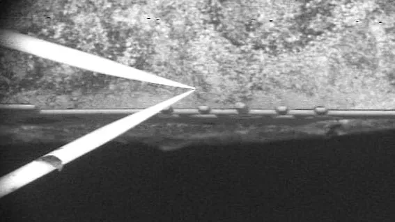
Cut out and lift microscopic, electron-transparent lamellae for transmission electron microscopy, faster, more accurately and more reliably.
Explore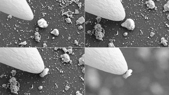 Materials Science
Nanomanipulation
Pick up, position and assemble nano-objects (wires, particles, flakes) inside the electron microscope.
Explore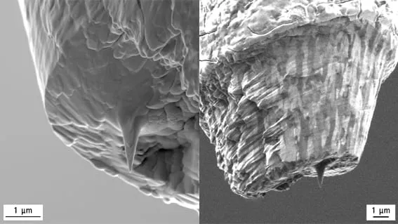 Materials Science
APT Sample Preparation
Shape and mount the needle-shaped specimens atom probe tomography needs, by in-situ FIB lift-out.
ExploreRelated publications
Aligned Stacking of Nanopatterned 2D Materials for High-Resolution 3D Device Fabrication
DOI 10.1021/acsnano.1c09122Mechanical cleaning of graphene using in situ electron microscopy
DOI 10.1038/s41467-020-15255-3Magnetic energies of single submicron permalloy rectangles determined via magnetotransport
DOI 10.1103/PhysRevB.80.134415Bottom-up Nanoconstruction by the Welding of Individual Metallic Nanoobjects Using Nanoscale Solder
DOI 10.1021/nl8025339Age determination of single plutonium particles after chemical separation
DOI 10.1016/j.sab.2008.10.044Exploring the conduction in atomic-sized metallic constrictions created by controlled ion etching
DOI 10.1088/0957-4484/19/41/415302Amplitude Response of Multiwalled Carbon Nanotube Probe with Controlled Length during Tapping Mode Atomic Force Microscopy
DOI 10.1021/jp804481gAccurate electrical testing of individual gold nanowires by in situ scanning electron microscope nanomanipulators
DOI 10.1063/1.3005423Integrated setup for the fabrication and measurement of magnetoresistive nanoconstrictions in ultrahigh vacuum
DOI 10.1063/1.2981693The Very Low Shear Modulus of Multi-Walled Carbon Nanotubes Determined Simultaneously with the Axial Young’s Modulus via in situ Experiments
DOI 10.1002/adfm.200701105Self-Retracting Motion of Graphite Microflakes
DOI 10.1103/PhysRevLett.100.0672053D failure analysis in depth profiles of sequentially made FIB cuts
DOI 10.1016/j.microrel.2007.07.032Forging of metallic nano-objects for the fabrication of submicron-size components
DOI 10.1088/0957-4484/18/12/125303A microdiffraction set-up for nanoporous metal–organic-framework-type solids
DOI 10.1038/nmat1991Cutting and sharpening carbon nanotubes using a carbon nanotube ‘nanoknife’
DOI 10.1088/0957-4484/18/18/185503Establishing Ohmic contacts for in situ current–voltage characteristic measurements on a carbon nanotube inside the scanning electron microscope
DOI 10.1088/0957-4484/17/4/041Design of a microgripping system with visual and force feedback for MEMS applications
Evaluation of different control algorithms for a micromanipulation system
Development and performance of the nanoworkbench: A four tip STM for conductivity measurements down to submicrometer scales
DOI 10.1063/1.1878213Controlled cleavage of single semiconducting nanowires and study on the suitability of their use as nanocavities for nanolasers
DOI 10.1063/1.1757635Transfer of a single particle for combined ESEM and TEM analyses
DOI 10.1016/S1352-2310(03)00574-0Performing probe experiments in the SEM
DOI 10.1016/j.micron.2003.12.005High-resolution nanowire atomic force microscope probe grown by a field-emission induced process
DOI 10.1063/1.1765202Fabrication of super-sharp nanowire atomic force microscope probes using a field emission induced growth technique
DOI 10.1063/1.1791321In-situ Lift-Out of TEM-Lamellae using a Compact and Precise Micromanipulator
Application articles
Introduction to APT sample preparation
Why atom probe tomography needs needle-shaped specimens, and how in-situ lift-out delivers them.
Introduction to TEM sample preparation
Why electron-transparent lamellae are hard to make, and how in-situ lift-out makes it routine.
What is nanomanipulation?
Moving, positioning and assembling individual nano-objects inside the electron microscope.
Preparing APT needles
Lift-out, mounting and annular milling, turning bulk material into a sharp atom-probe specimen.
The in-situ lift-out workflow
Approach, attach, cut free, transfer and mount, the choreography of a clean FIB lift-out.
Two-arm handling & assembly
Using two or more manipulators together to hold, hand off and assemble nanoscale parts.
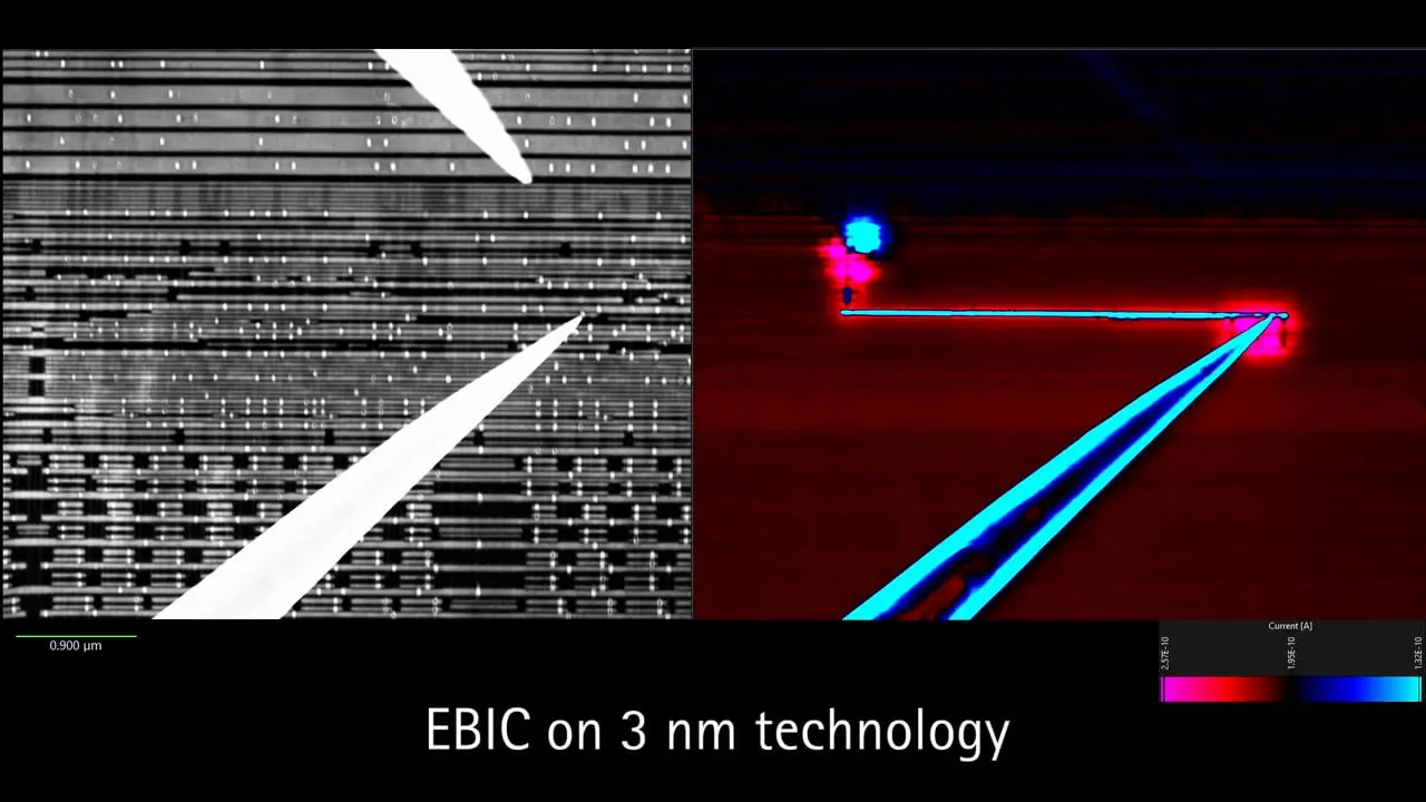
EBIC — Electron-Beam-Induced Current
Mapping where a device collects beam-generated carriers, to image p–n junctions, depletion regions and recombination sites.
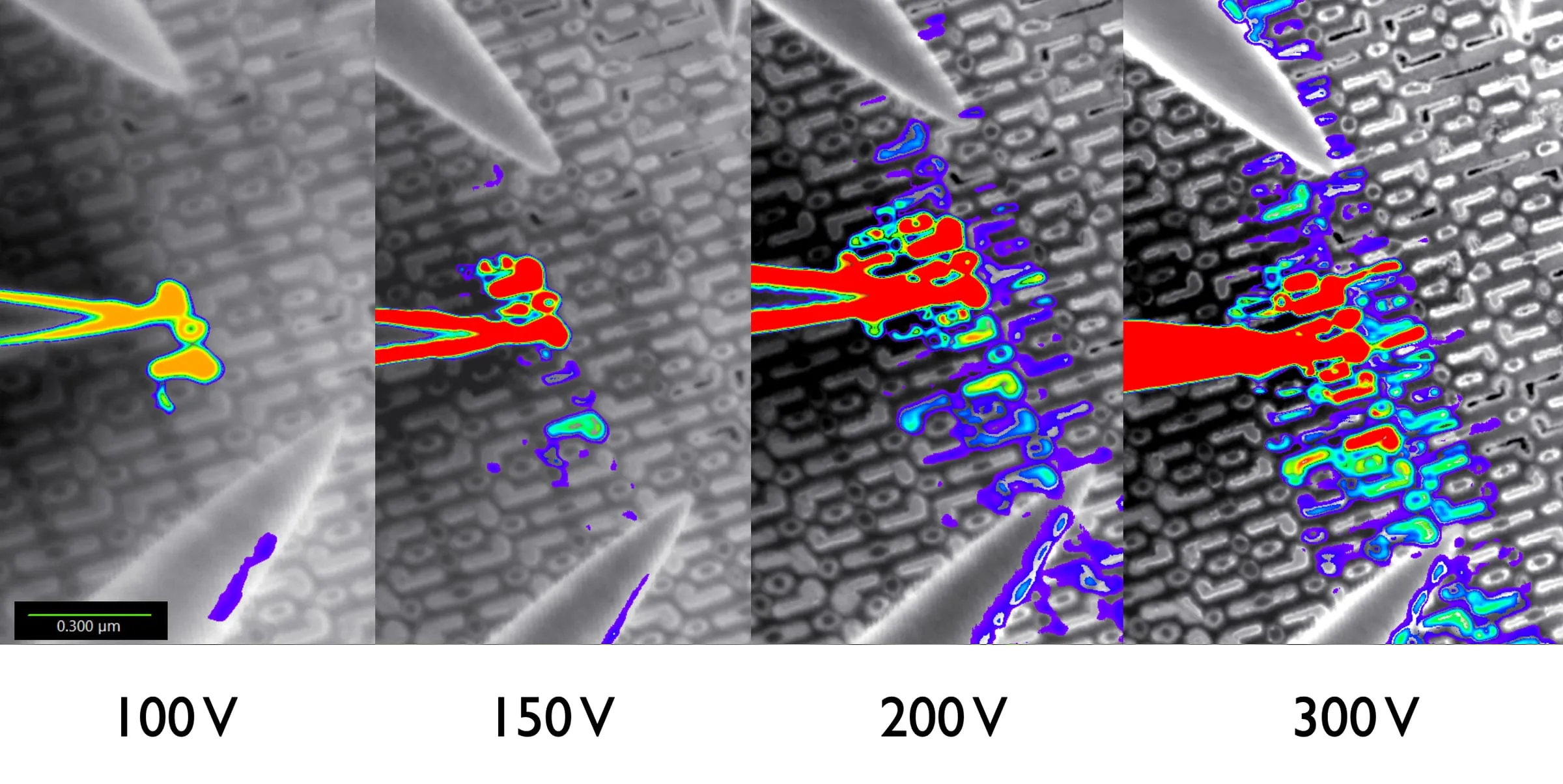
EBAC — Electron-Beam Absorbed Current
Tracing conductive paths and finding opens in interconnects, with no bias applied to the device.
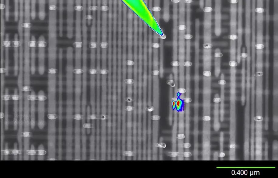
RCI — Resistive Contrast Imaging
Two-contact current-division imaging that reveals the resistance distribution along a net.
EBIRCH — Electron-Beam-Induced Resistance Change
Biased, AC current imaging that lights up resistive and leaky defects as bright spots.
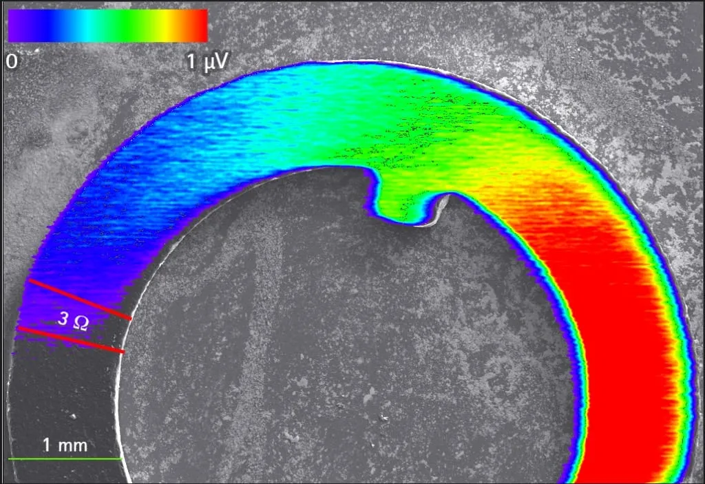
EBIV — Electron-Beam-Induced Voltage
Reading the beam-induced voltage to reach high-impedance and floating nodes that current maps miss.
Lift-out, filmed inside the chamber
Full TEM lamella lift-outs and the iLO control software, recorded under the beam.
Nanomanipulation in the microscope
Pick-and-place and nanowire handling, filmed inside the SEM.
Related products & accessories
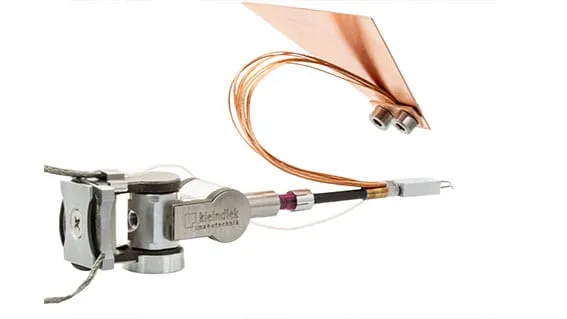
Cryo Lift-Out (CryoLO)
Cryogenic in-situ TEM-lamella lift-out — a cryoMGS-EM microgripper cooled to LN₂ temperature while the MM3A-EM itself stays at room temperature.
View product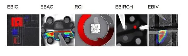
EBIC Amplifier
A low-noise current amplifier that turns the electron beam into a defect-mapping tool — EBIC, EBAC, RCI, EBIRCH and EBIV from a single unit.
View product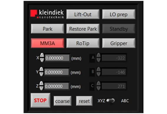
iLO Control Software
The graphical lift-out control software — drag-and-drop positioning with automatic beam, rotation and magnification compensation.
View product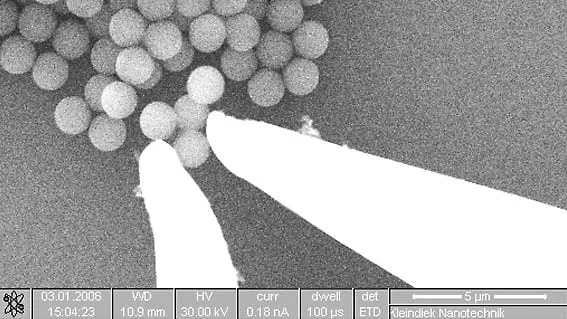
Micro Gripper MGS2
A two-jaw micro-gripper that picks up, holds and repositions micro-objects inside the electron microscope.
View product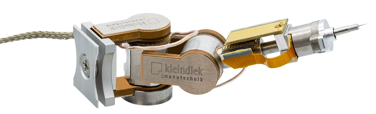
MM3E
An encoded, closed-loop micromanipulator — define parking and working positions and recall them at the click of a button.
View product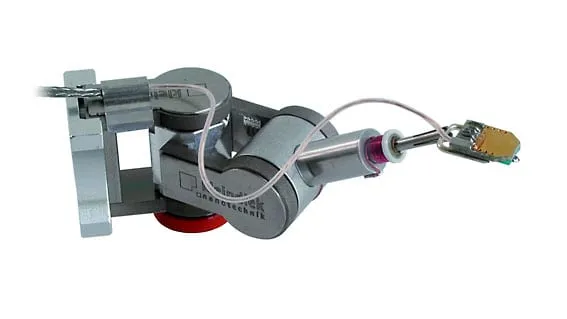
Force Measurement System FMS
Laser-free force measurement and nanoindentation in the SEM — resolve forces to 10 nN and identify materials by their resonance.
View product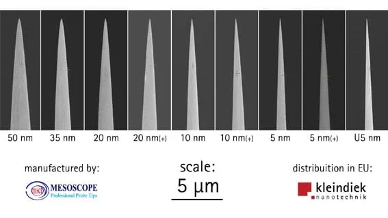
Mesoscope Probe Tips
High-end tungsten probe tips with radii from 250 nm down to 5 nm — ready to probe straight from the pack.
View product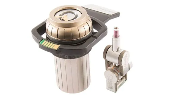
MM3A-EM for Phenom
The MM3A-EM micromanipulator integrated into the Phenom desktop SEM — add a needle, microgripper or force sensor to your benchtop instrument.
View product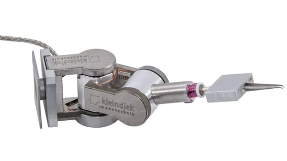
Microtweezer MTW
A piezo-driven microtweezer for pick-and-place — one jaw fixed, one jaw stepping in 0.25 nm increments across a 3 mm span.
View product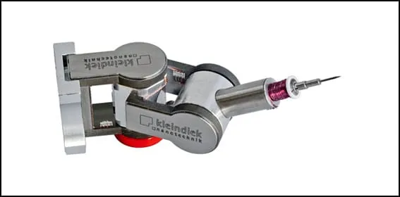
MM3A-LMP
An economical, flexible probe-station manipulator for electrical measurements on 45–90 nm and larger technology nodes.
View product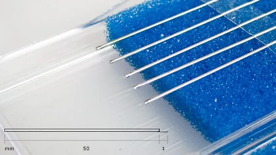
PicoProbe Tips
Tungsten probe tips for everyday probing — most commonly 100 nm radius, packaged under protective atmosphere.
View product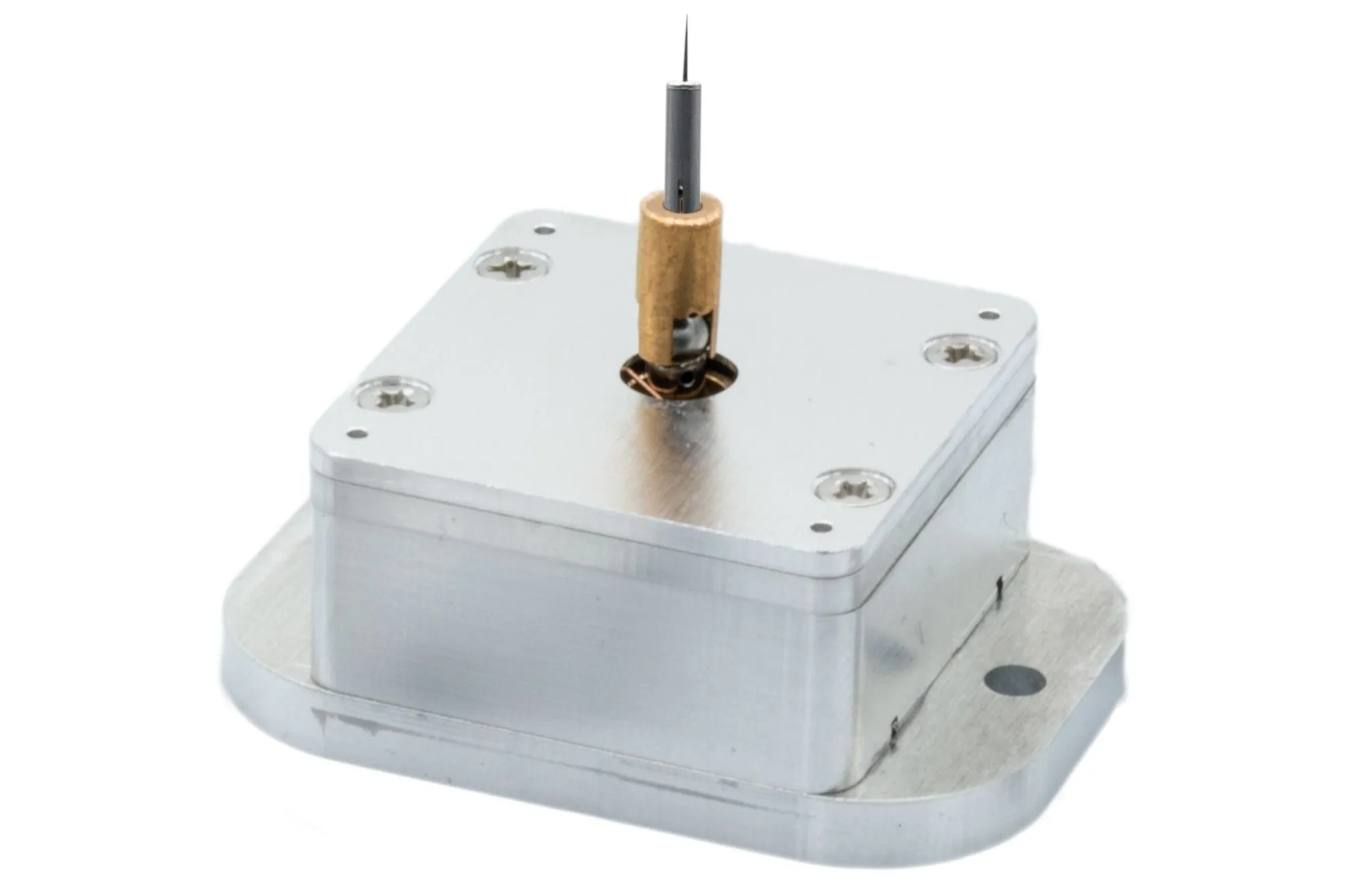
Nanolathe (RT-LATHE)
A stand-alone rotational axis for true FIB lathe milling and tomography — spin a region of interest concentrically under the beam.
View product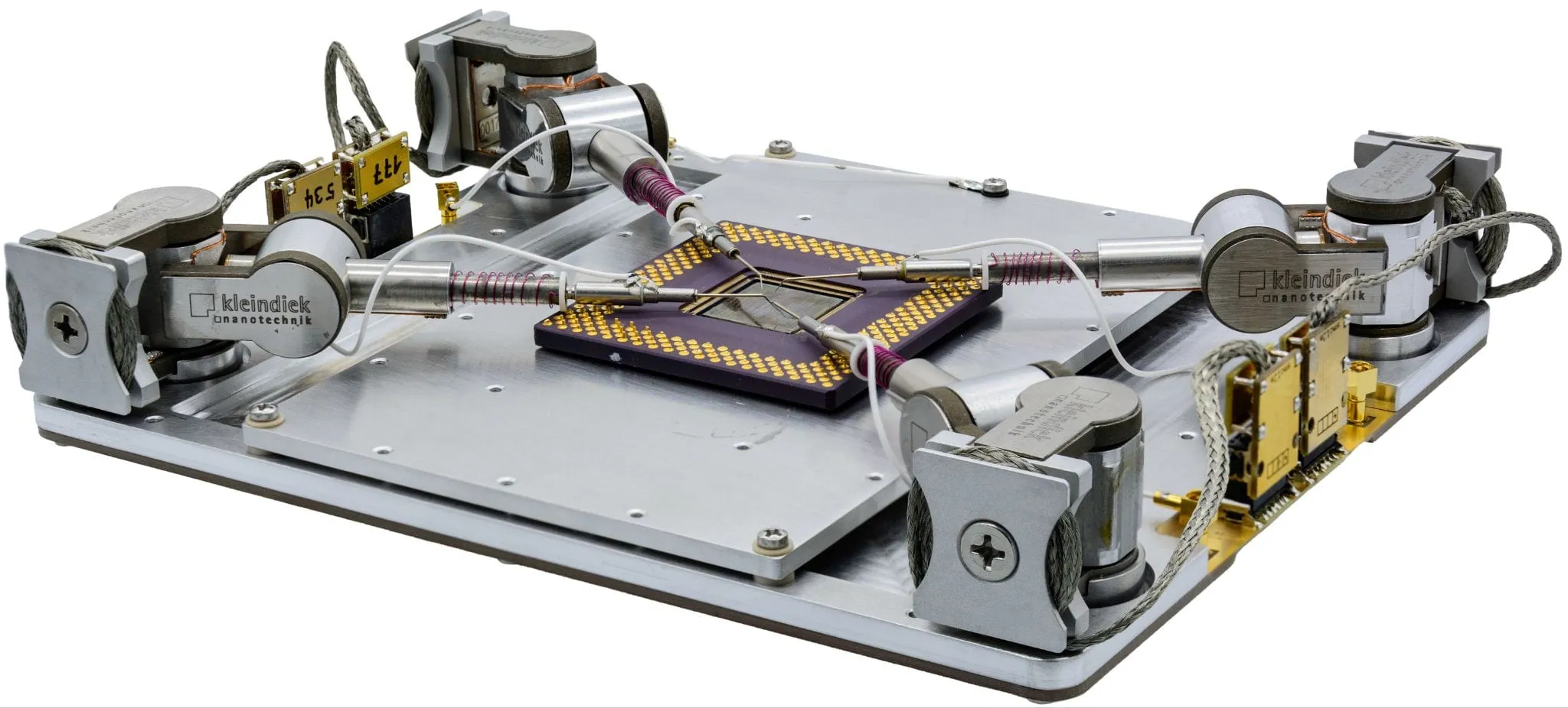
NW4
A load-lock platform hosting up to four MM3A-EM manipulators — nanoprobing and failure analysis on large substrates up to 120 × 120 mm.
View product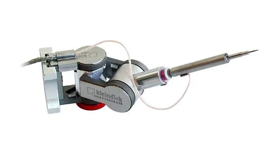
RoTip
A rotational-axis plug-in that adds a fourth degree of freedom — continuous 0.1° rotation for true FIB lathe milling, tomography and STEM.
View product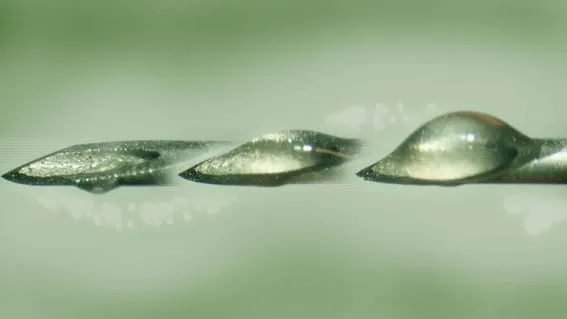
SemGlu
A high-vacuum adhesive that cures only where you focus the beam — epoxy-grade bonds for in-SEM assembly and lift-out.
View product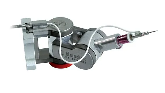
Probe-Tip Holder LCMK
A low-noise, low-resistance probe-tip holder that turns a Kleindiek manipulator into a precision nanoprober — resolving currents down to 3 fA.
View product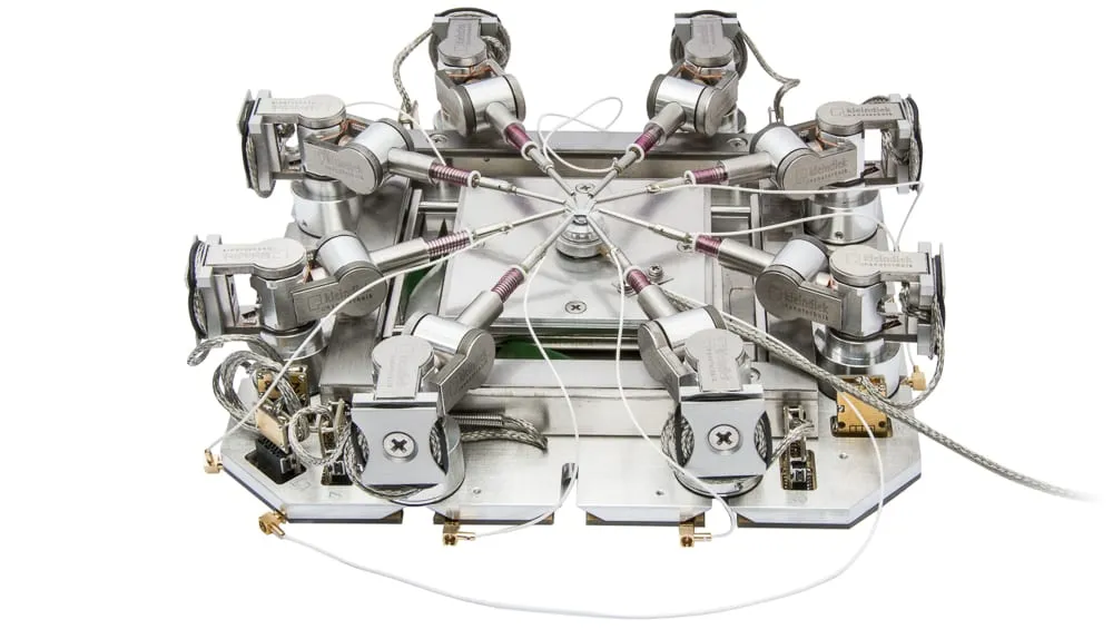
ProbeWorkstation+
Up to eight manipulators, a roof-mounted prober and a 30 mm substage — a complete in-SEM probe station, installed or removed in 60 seconds.
View product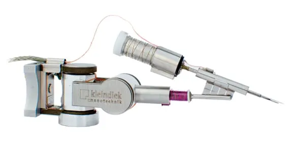
Gas Injection System GIS
A gas-injection plug-in that meters precursors and gases into the SEM chamber in precise doses, through a proportional valve driven by a Nanomotor®.
View product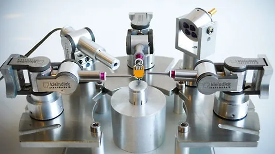
SemCam
An in-chamber CCD camera that watches the probe approach from the side — land tips in under thirty seconds.
View product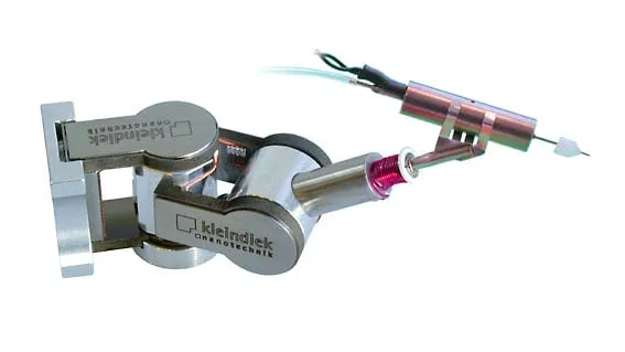
Microinjection System MIS
A micro-valve plug-in for precise microinjection of liquids onto samples in the low-vacuum SEM, down to roughly 100 µm droplets.
View product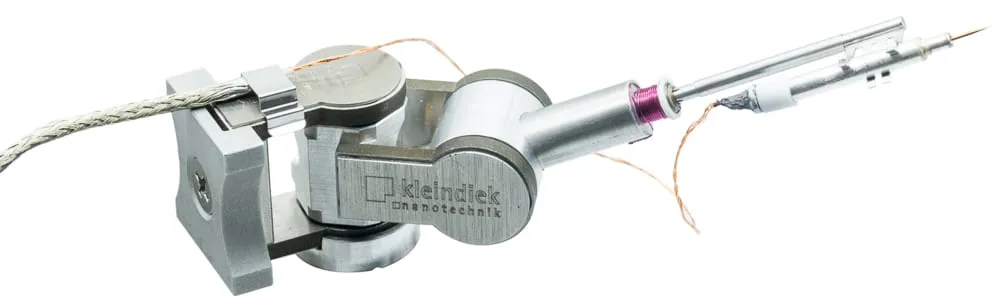
Micro Soldering Unit MSU
A miniaturized, closed-loop soldering iron for the SEM — set a tip temperature and hold it, in air or in vacuum, for micro-scale joining.
View productTalk to an application engineer
Tell us your sample and your microscope — we’ll walk you through the workflow and route you to the right regional team.