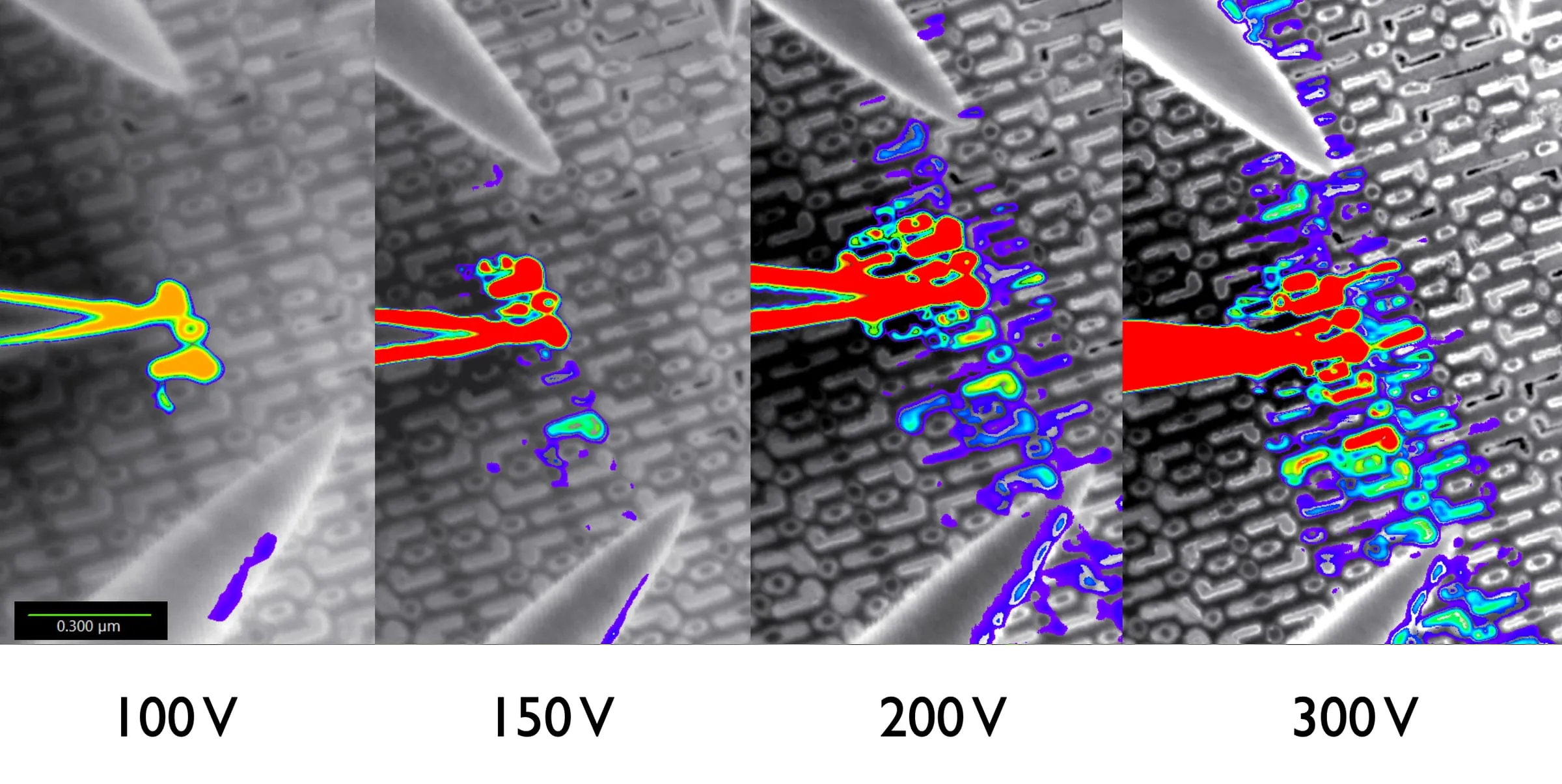
Resistance between the beam spot and the probe#
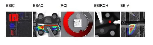
EBAC reads the current absorbed by a conductor as the electron beam scans across it. With a probe attached to one end of an interconnect, the absorbed current depends on the resistance between the beam spot and the probe, so a continuous metal line images as a smooth gradient, while a break or high-resistance segment appears as an abrupt change in contrast at its exact location.
One probe, and no bias on the device#
A single probe contacts the net of interest and the EBIC amplifier reads the absorbed current, mapping it onto the secondary-electron image. Crucially, no bias is applied to the device, which makes EBAC a gentle technique well suited to passive interconnect structures and to nets that must not be electrically stressed.
Opens, broken lines and buried paths#
Localizing opens, broken interconnects and high-resistance vias, and tracing buried conductive paths through multilevel metal, a fast first step in interconnect failure analysis.