Before you land probes, current imaging tells you where to look. By scanning the electron beam and reading the current it induces or that flows through the device, you build a map of electrical activity and pinpoint the defect, turning a needle-in-a-haystack search into a targeted measurement.
The current-imaging family#
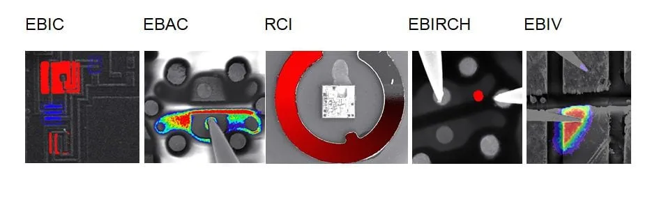
- EBIC (Electron-Beam-Induced Current). The beam generates electron–hole pairs; junctions and depletion regions collect them, revealing p–n junctions and recombination sites.
- EBAC (Electron-Beam Absorbed Current). Reads the current absorbed by an interconnect, mapping conductive paths and breaks without biasing the device.
- EBIRCH (Electron-Beam-Induced Resistance Change). Localizes resistive faults and shorts by imaging beam-induced resistance changes under bias.
- RCI (Resistive Contrast Imaging). Two contacts split the beam-injected current by resistance, exposing opens and resistive defects along a net.
- EBIV (Electron-Beam-Induced Voltage). Maps the beam-induced voltage at a probe, a complementary view for connectivity tracing.
Why it pairs with nanoprobing#
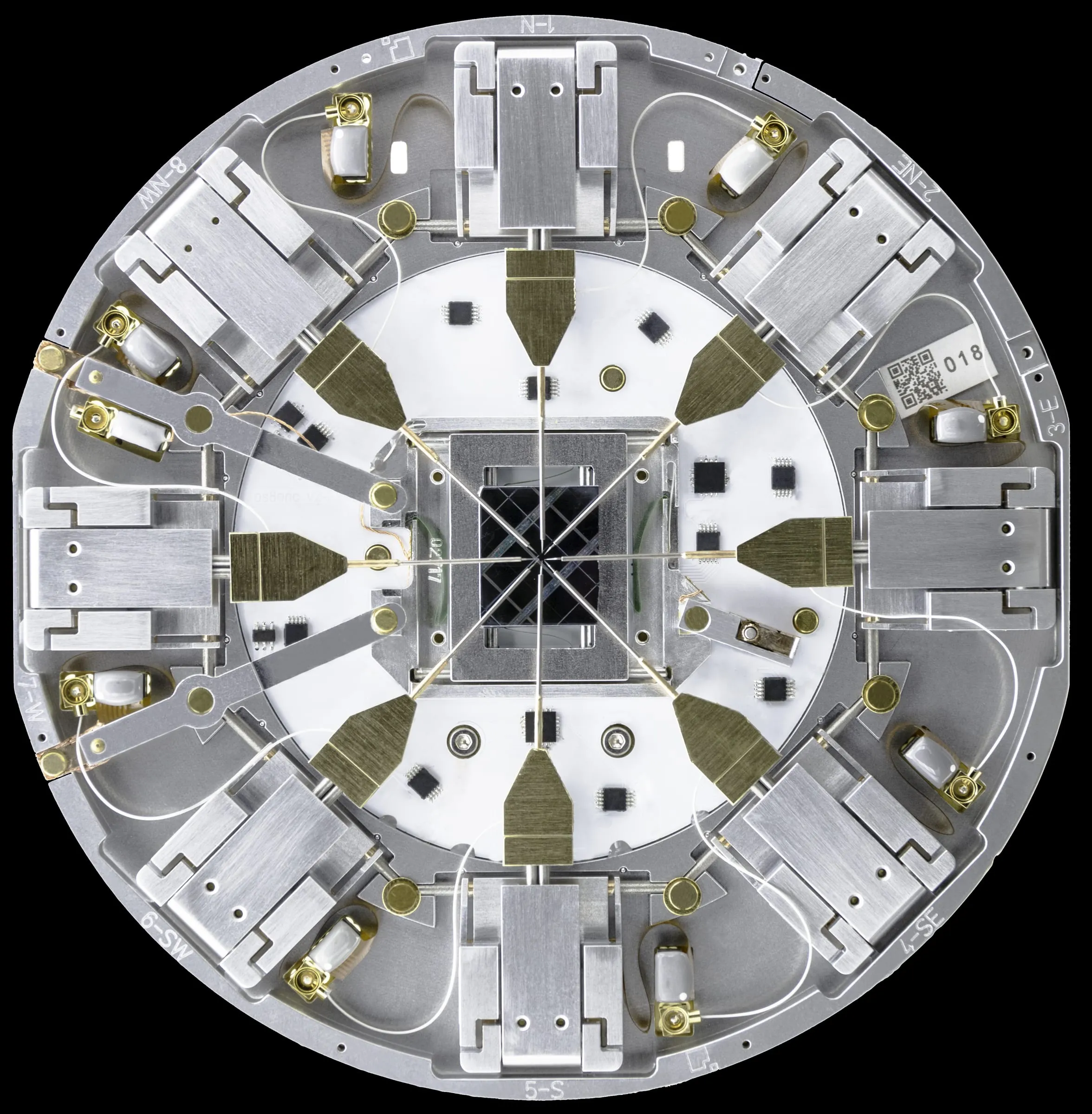
The Prober Shuttle’s probes double as the contacts for current imaging, so a single setup handles both mapping (EBIC/EBAC/EBIRCH) and quantitative I–V probing without re-instrumenting between steps.
Deep dives#
Each technique has its own article: EBIC, EBAC, RCI, EBIRCH and EBIV.