Voltage, not current#
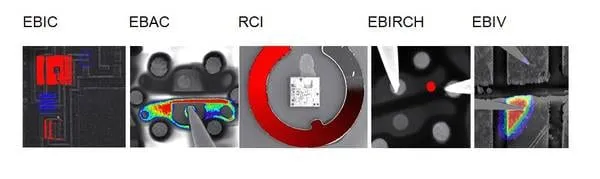
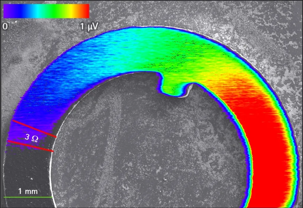
EBIV records the voltage the electron beam induces at a probe, rather than the absorbed current. As the beam injects charge at each scan position, the potential it raises at the probe depends on how that point is connected through the net, so the resulting map traces conductors, contacts and discontinuities from the voltage side rather than the current side.
One probe, passivation left in place#
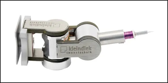
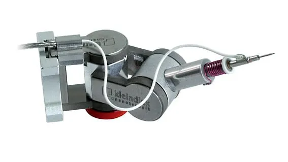
A probe contacts the net, and the EBIC amplifier reads the induced voltage and maps it onto the secondary-electron image, again with the passivation left in place.
Reaching floating and high-impedance nodes#
Voltage sensing draws essentially no current, so EBIV reaches nodes where current-based methods struggle: high-impedance paths and floating structures that cannot carry a measurable absorbed current. On those, it localizes opens and leakage from the voltage side, where a current map would read flat.