
Prober Shuttle PS8
High-precision in-situ electrical nanoprobing with up to eight ultra-flat MM4 manipulators — for advanced-node failure analysis.
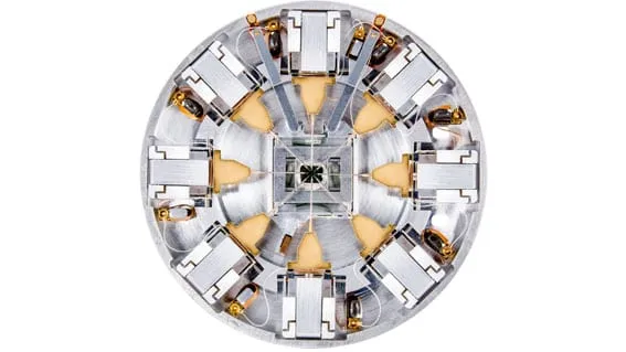
Eight probes, twenty-seven axes#
Where the PS8e adds encoders, the PS8 is the platform they were built on: a 140 mm diameter, 10 mm tall shuttle carrying up to eight ultra-flat MM4 three-axis manipulators plus a three-axis substage — 27 axes of motion in total, each resolving linear moves below 0.02 nm. Every manipulator’s Z drive swings up 90° for clear access to the sample and tool-free exchange of probe tips, and each carries its own low-noise triax connector so weak signals stay clean from tip to rack.
Built for the failure-analysis lab#
The whole platform loads into the chamber through a 6 inch load lock, so swapping samples doesn’t mean venting the SEM — cycle times stay short and throughput stays high. Manual probe placement, guided by the same 0.02 nm-class positioners as the PS8e, keeps the PS8 rated for the 7 nm node and beyond; step up to encoded pre-alignment on the PS8e when low-kV imaging across all eight probes becomes the bottleneck. Add the optional Advanced Probing Tools suite (Live Contact Tester, Electron-Beam-Induced-Current EBIC/EBAC imaging) and the PS8 covers most in-situ electrical characterization work in the lab. Non-magnetic construction and FIB-angle tilt round out a platform built to retrofit onto an existing stage.
Gallery
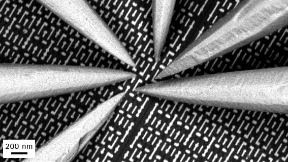
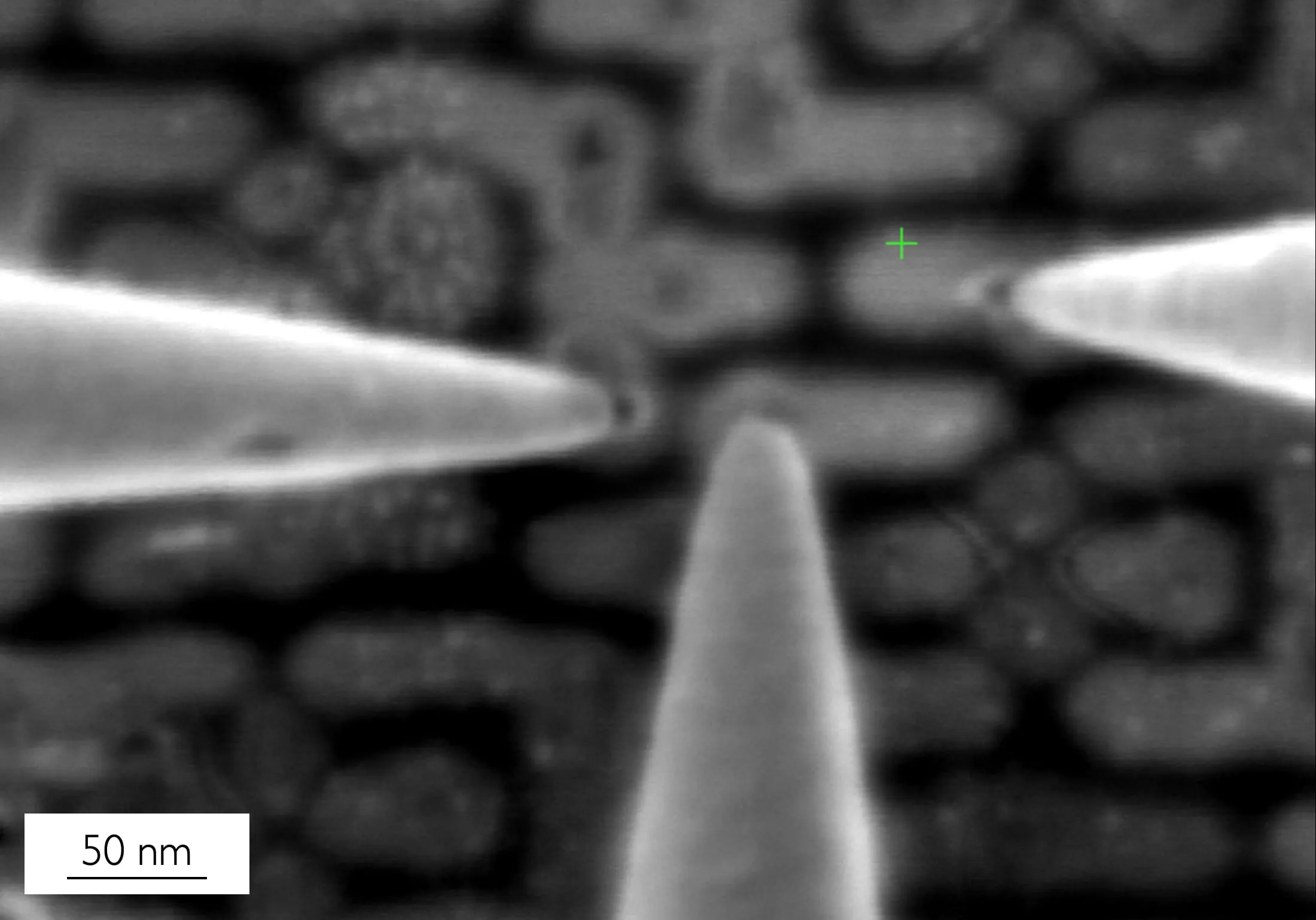
Six tips landed on a patterned surface — 200 nm scale bar. 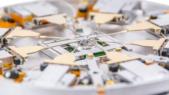
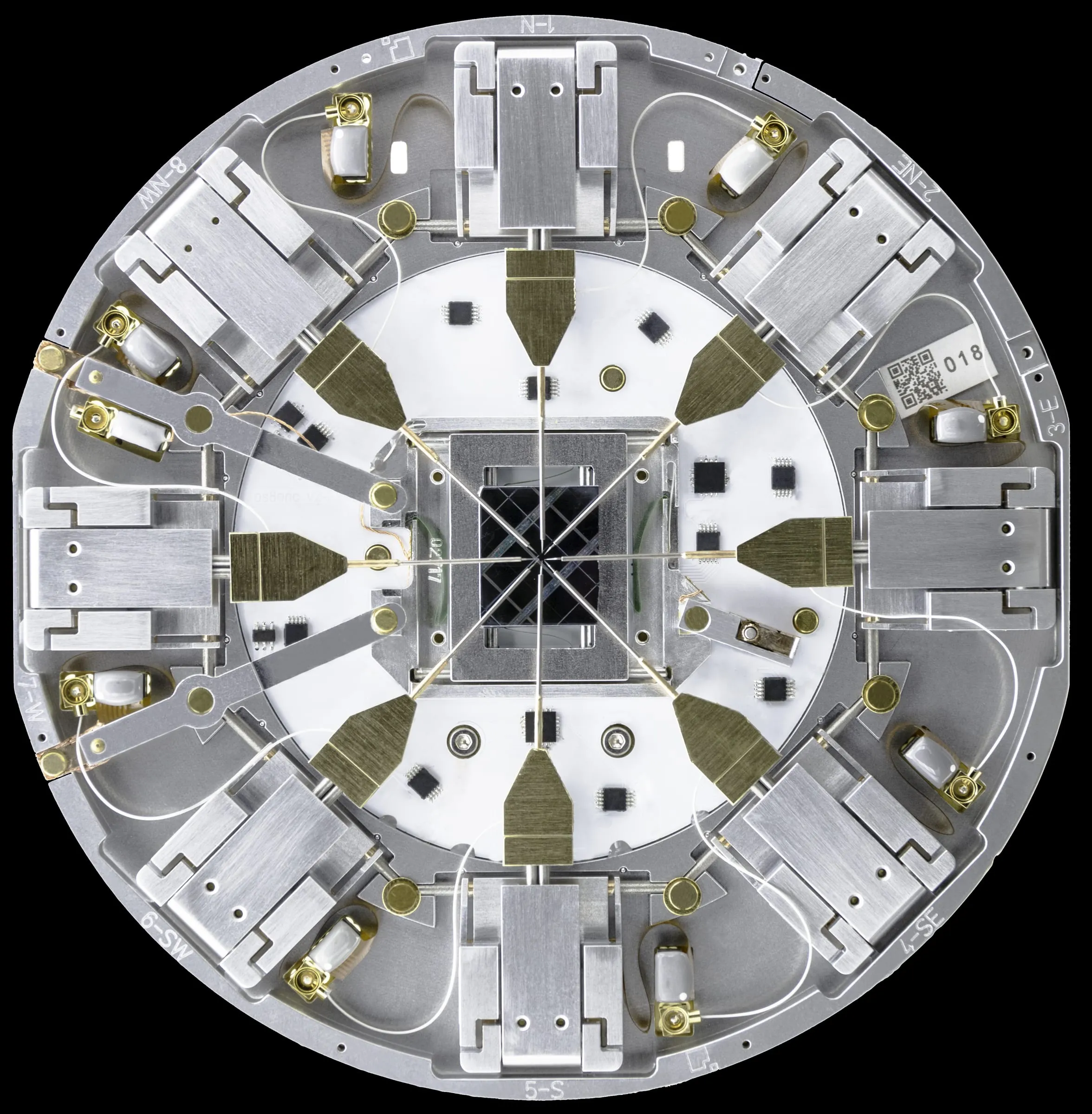
The 140 mm platform fully populated with eight MM4 manipulators. 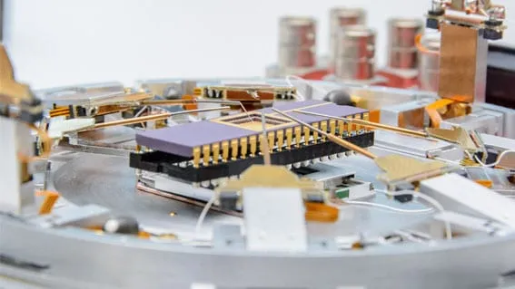
A packaged device mounted on the substage, ready for probing. 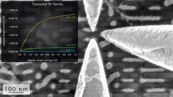
Transistor I–V family acquired in situ, overlaid on the landed probes.
Technical data
Overview
- Diameter
- 140 mm
- Total height
- 10 mm
- Max. sample area
- 20 × 20 mm
- Max. sample height
- 20 mm
- Manipulators
- up to 8 × MM4
Substage
- Travel — X / Y
- 9 mm
- Travel — Z
- 0.7 mm
Motion (per manipulator)
- Range — A / C
- 5 mm
- Range — B (rotation)
- 90°
- Resolution — A / C
- < 0.02 nm
- Resolution — B
- < 0.5 nm
- Max. velocity
- up to 1 mm/s
- Drift
- < 1 nm/min
Electrical
- Max. voltage
- 100 V
- Max. current
- 100 mA
- Noise
- 20 fA @ 1 Hz
- Insulation leakage — probes
- < 50 fA/V
- Insulation leakage — sample
- < 150 fA/V
- Signal conductor resistance
- < 5 Ω
See it run
Advantages
Same platform, manual control
- 27 axes across eight MM4 manipulators and the three-axis substage, each resolving below 0.02 nm
- Every manipulator's Z drive swings up 90° for direct access and probe-tip changes without tools
- Low-noise triax connector on every manipulator for clean low-current signals
Built for the failure-analysis lab
- 6 inch load-lock compatible platform for short cycle times and high sample throughput
- Rated for the 7 nm node and beyond
- Compatible with the Advanced Probing Tools suite, including Live Contact Tester and EBIC/EBAC imaging
Easy to integrate
- 19-inch rack electronics stay outside the chamber and out of the operator's sightline
- Non-magnetic construction; tilts to the FIB angle for circuit-edit work
- Plug-and-play, modular components drop onto an existing sample stage
Application articles
What is nanoprobing?
How in-situ probing measures the electrical behaviour of individual transistors at the most advanced nodes.
EBAC — Electron-Beam Absorbed Current
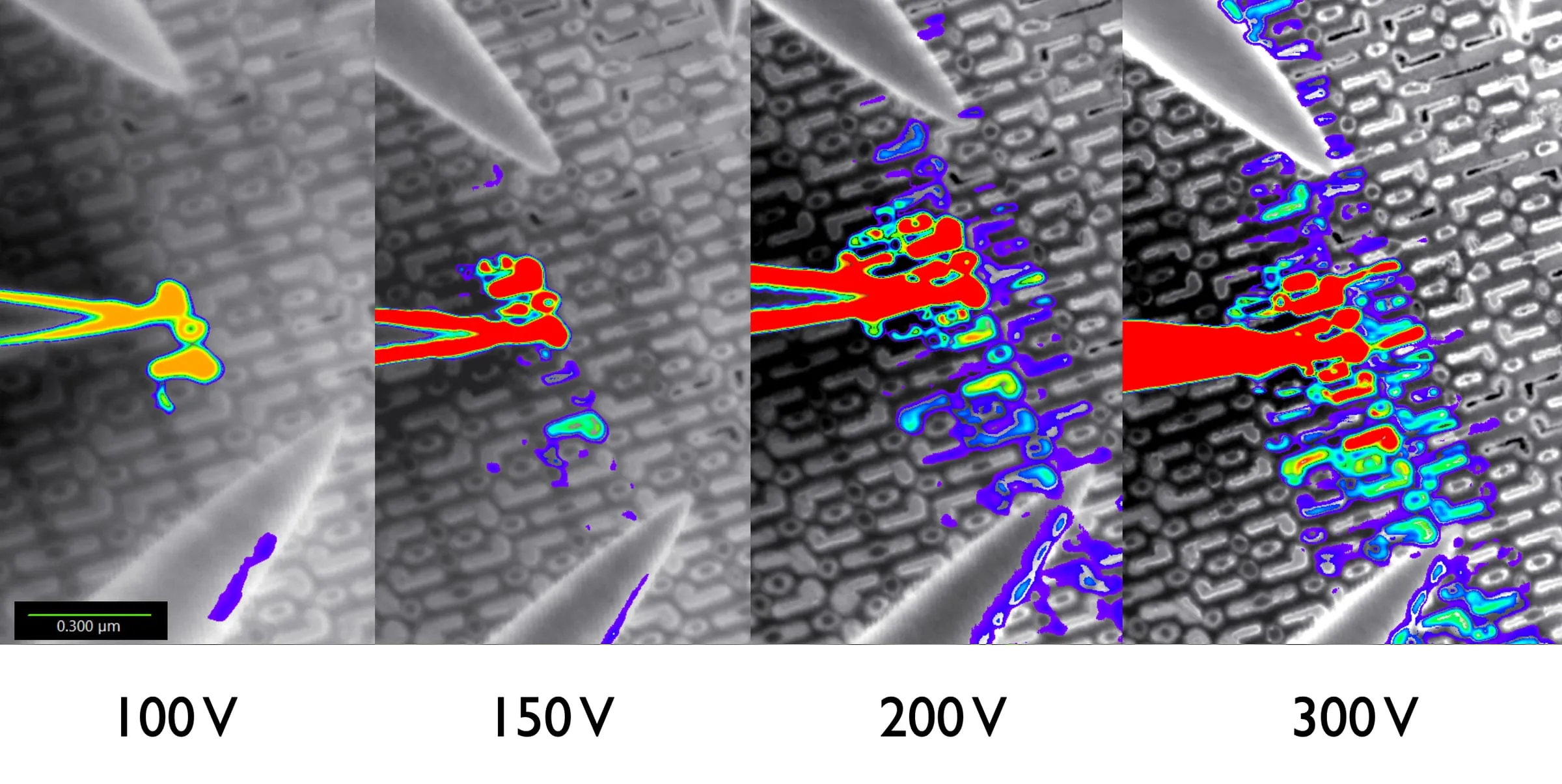
Tracing conductive paths and finding opens in interconnects, with no bias applied to the device.
EBIRCH — Electron-Beam-Induced Resistance Change
Biased, AC current imaging that lights up resistive and leaky defects as bright spots.
Nanoprobing in the microscope
In-situ nanoprobing and failure analysis, filmed inside the SEM, from probe landing to live I–V curves.
Related products & accessories
Prober Shuttle PS8e
A compact, fully integrated nanoprobing system — now encoded for automatic probe pre-alignment. Optimized for the 3 nm node and beyond.
View product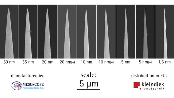
Mesoscope Probe Tips
High-end tungsten probe tips with radii from 250 nm down to 5 nm — ready to probe straight from the pack.
View product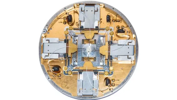
Prober Shuttle PS4
A compact two- or four-probe nanoprobing system for in-situ electrical characterization at advanced nodes.
View product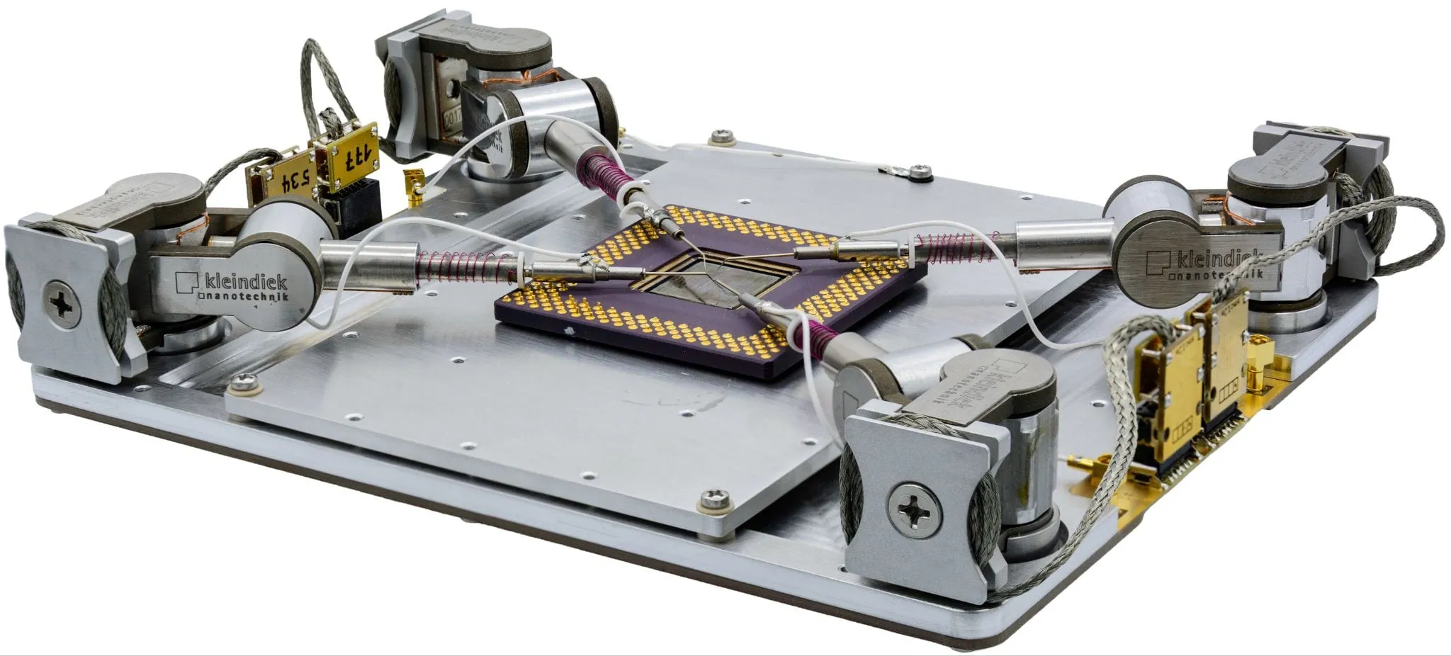
NW4
A load-lock platform hosting up to four MM3A-EM manipulators — nanoprobing and failure analysis on large substrates up to 120 × 120 mm.
View product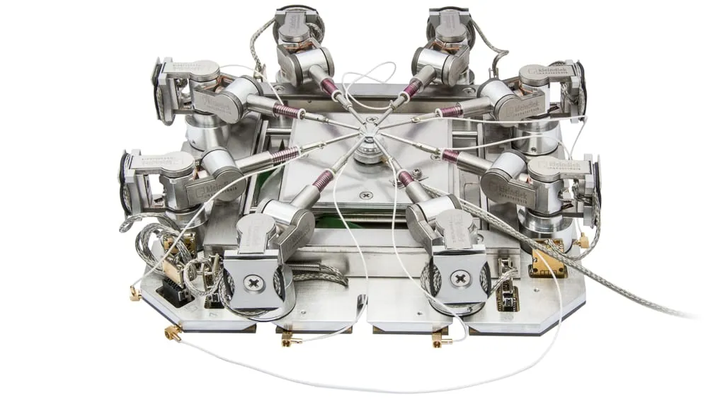
ProbeWorkstation+
Up to eight manipulators, a roof-mounted prober and a 30 mm substage — a complete in-SEM probe station, installed or removed in 60 seconds.
View product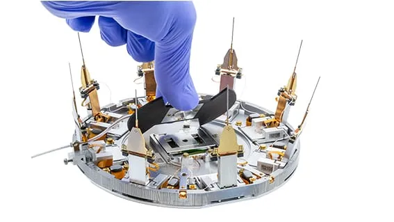
Heating & Cooling Stage for PS8
A heated/cooled stub for the Prober Shuttle PS8 — regulate sample temperature from −20 °C to +150 °C during probing, water-cooling-free.
View productTalk to an application engineer
Tell us your sample and your microscope — we’ll walk you through the workflow and route you to the right regional team.