
NW4
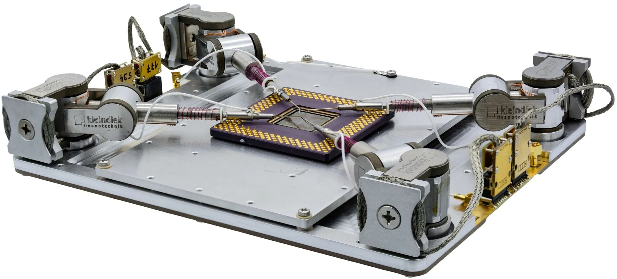
A load-lock platform hosting up to four MM3A-EM manipulators — nanoprobing and failure analysis on large substrates up to 120 × 120 mm.
Built for packaged parts#
Most nanoprobing platforms stop at die level. The NW4 covers the other end of the failure-analysis workflow: packaged devices and other large substrates up to 120 × 120 mm, with sample thicknesses up to 30 mm depending on how the load lock is used. Up to four MM3A-EM micromanipulators surround the sample, each on a low-noise signal lead, with a further low-noise lead for the sample or bulk; the measurement chain resolves currents down to 3 fA at 1 Hz. How much of that area the beam can image depends on your chamber dimensions.
Tips and samples through the load lock#
The load-lockable base lets you exchange samples and replace probe tips without breaking vacuum in the main chamber, keeping cycle times short and contamination low. And because the whole platform rides the microscope stage, you can land a probe and then track EBIC or EBAC traces between sites far apart on the substrate.
Drop-in partner for the PS8#
The NW4 uses the same vacuum-side hardware, mounting and connector as the Prober Shuttle PS8 — down to the same air-side controllers — so the two platforms swap in and out of one microscope. Run them in alternation and a single tool set covers everything from the most recent nodes to packaged samples.
Gallery
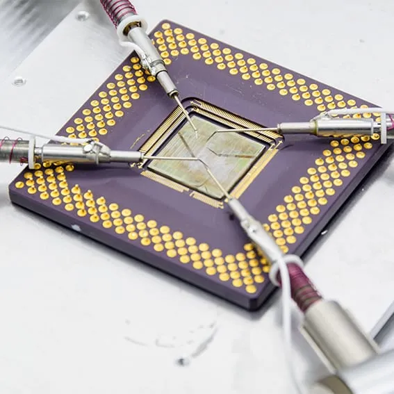
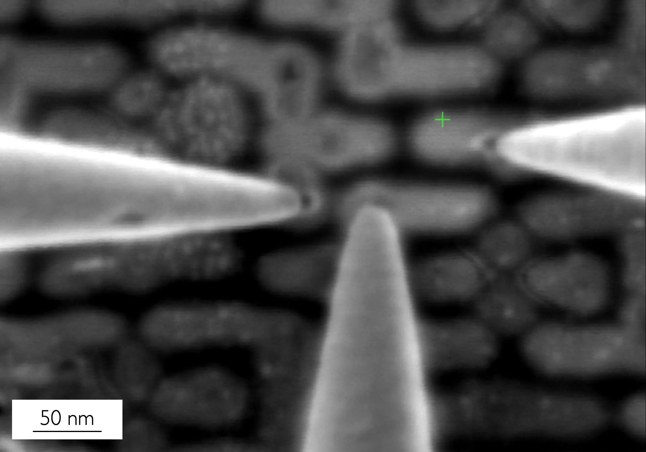
Four probes on a decapsulated package — the NW4 accepts substrates up to 120 × 120 mm. 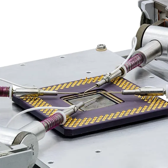
Package FA in progress on the 162 × 134 mm platform. 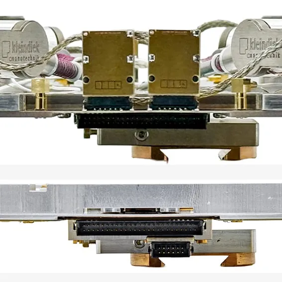
The same connector as the Prober Shuttle PS8 — the two platforms swap without rewiring.
Technical data
Platform
- Platform dimensions
- 162 × 134 mm
- Max. substrate size
- 120 × 120 mm
- Max. substrate thickness
- 30 mm (very large substrates may be limited to 6 mm)
- Manipulator capacity
- up to 4 × MM3A-EM
- Load lock
- Compatible
- Connector
- Same as Prober Shuttle PS8
Low-current measurement
- Current measurement limit
- 3 fA @ 1 Hz
- Insulation leakage
- 50 fA @ 1 V
- Signal conductor resistance
- 6.5 Ω
- Max. voltage
- 210 V
- Max. current
- 200 mA
Three-axis micromanipulators
- Range — A & B
- 240°
- Range — C
- 12 mm
- Speed — A & B
- up to 10 mm/s
- Speed — C
- up to 2 mm/s
- Resolution — A
- 0.35 nm (7 nrad)
- Resolution — B
- 0.25 nm (7 nrad)
- Resolution — C
- 0.05 nm
- Dimensions
- 62.1 × 20.4 × 25.4 mm, 45 g
- Lowest pressure
- 10⁻⁷ mbar
- Drift
- 1 nm/min
Advantages
Package FA on large substrates
- Probes packaged devices and substrates up to 120 × 120 mm
- Accepts samples up to 30 mm thick, depending on load-lock use
- Hosts up to four MM3A-EM manipulators on a 162 × 134 mm base
- Low-noise signal leads for all four probes plus the sample/bulk
Probe exchange without breaking vacuum
- Load-lockable base for sample exchange and tip replacement
- Keeps cycle times short and the main chamber clean
- The platform rides the microscope stage, so a landed probe can follow EBIC/EBAC traces across the substrate
Drop-in partner for the PS8
- Same vacuum-side hardware, mounting and connector as the Prober Shuttle PS8
- Runs from the same air-side controllers, so the two platforms alternate in one tool
- Together they span die-level nodes to packaged parts
Low-current measurement
- Resolves currents down to 3 fA at 1 Hz
- Insulation leakage of 50 fA at 1 V
- Signal conductor resistance of 6.5 Ω
- Up to 210 V and 200 mA
Related products & accessories
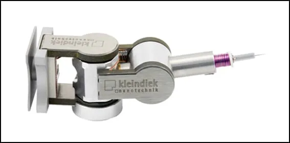
MM3A-EM
The industry-standard spherical micromanipulator — the platform every Kleindiek plug-in tool attaches to, with 3000+ units in the field.
View product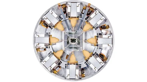
Prober Shuttle PS8
High-precision in-situ electrical nanoprobing with up to eight ultra-flat MM4 manipulators — for advanced-node failure analysis.
View productTalk to an application engineer
Tell us your sample and your microscope — we’ll walk you through the workflow and route you to the right regional team.