Aligned Stacking of Nanopatterned 2D Materials for High-Resolution 3D Device Fabrication
Highlight
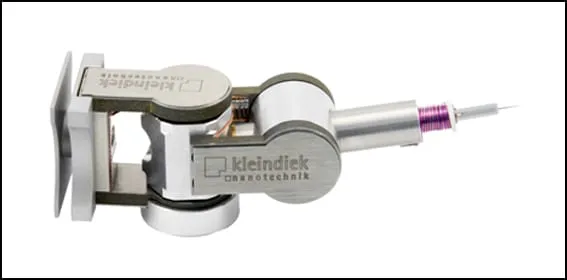
Stacking nanopatterned 2D-material sheets with micrometre alignment, a Tübingen team built 3D devices layer by layer, placing each sheet with an MM3A-EM.
This work assembles three-dimensional device architectures by stacking individually nanopatterned 2D-material flakes with high lateral alignment. An MM3A-EM provides the micrometre registration, positioning each patterned layer relative to the last and turning sheet-by-sheet assembly into a route for high-resolution 3D nanofabrication.